
 NextPCB Capabilities
Printed Circuit Boards
NextPCB Capabilities
Printed Circuit Boards
 PCB Assembly
 Layer Buildup
 SMD-Stencils
 PCB Design-Aid & Layout
 Mechanics
 Quality
 Drills & Throughplating
 Factory & Certificate
 PCB Assembly Factory Show
Certificate
PCB Assembly Factory Show
Certificate
Support Team
Feedback:
support@nextpcb.com


When selecting the number of layers of the board, some customers may ask: Why is the "number of layers of the board" option mostly even? You can not choose an odd number?
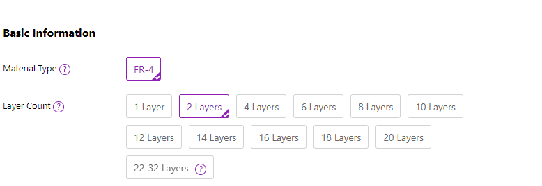
Theoretically speaking, PCB manufacturers can process the multilayers in odd and even numbers as long as within the process capability.
However, whether online or offline, only order numbers are large enough or customers are willing to pay enough money, PCB foundries are willing to accept odd-layer boards. Otherwise, they generally do not receive.
Here are the main three reasons to choose layers in even numbers: manufacturing cost, time cost, and quality.
First, odd-layer PCBs need to add a non-standard laminated core layer bonding process on top of the nuclear structure process, so the processing cost of odd-layer PCBs is significantly higher than even-layer PCBs.
Second, for many foundries, even-layer PCBs are general designs, while odd-layer PCBs are special designs. The special design means that it needs to be paired with a special production process, matching specific or even completely different production parameters, which requires a lot of trial and error costs.
Finally, the special design is often not the common process of the PCB Manufacturer. So production often requires the designation of experienced engineers dedicated to following up resulting in the rise of labor costs. And the successful implementation of special design also requires production, process, quality, and other departments to discuss together and work together, otherwise, it is easy to make mistakes.
All of the above, results in a very high cost of special design boards. So the odd-layer boards will be far more expensive than the conventional even-layer boards, which in turn leads to customers not accepting odd layers, choosing to use conventional even-layer.
Related Article: PCB cost: How Much Does a Printed Circuit Board (PCB) Cost?

In addition to the monetary cost, odd-layer boards take more time to produce than even-layer boards in practice.
On the one hand, the special design means that it has a lot of places where the usual familiar production is not the same. For odd-layer PCBs, PCB manufacturers need to do a lot of targeted pre-arrangement to ensure smooth production. And more preparation work will take more time.
On the other hand, the special design is a new process to work. So the factory workers will be very unskilled, leading to further lengthening of production time.
So maybe the fastest lead time for a 4-layer board with a universal design is only 2 days (like NextPCB), but for a 5-layer board with a special design, it takes 5 days, or even longer. Therefore, special design products in large quantities, even if the PCB manufacturer is willing to take the order, customers themselves often give up because of the long delivery time.
For an odd layer such as a special design of the board, the above-mentioned cost and time factors can be solved with money and patience. But the most important PCB quality is not ensured.
To ensure quality is the best reason for not using odd-layer design PCBs:
Reason 1: odd-layer PCBs are easier to bend. When the PCB is cooled by the multilayer bonding process, the PCB bends due to inconsistent lamination tension between the core structure and the foil-laying structure. The key to eliminating bending is to use a balanced stack of layers, and even if layers of PCB are symmetrical, the degree of warpage can be controlled to less than 0.7%. But odd-layer PCB, especially when the size is large, warpage will exceed 0.7%.
Reason 2: Even-number of layers of the stacked design is conducive to improving the PCB anti-interference ability. PCB signal layer and ground layer (or power supply layer) generally appear in pairs, which can shield the device signal interference. Such as the common 6-layer board layer order: SIG-GND-SIG-PWR-GND-SIG.
Reason 3: A core board is copper on both sides which can draw lines, made into an odd number of layers means that there is a wasting empty one. Therefore, for any EMI engineer, this layer will be designed as a power layer or ground layer to play a shielding role.
In addition, special processes are difficult to ensure the yield, so the yield of odd-layer PCBs tends to be lower than the even layer. Moreover, it is also difficult to ensure quality control without defects in the production process. Regardless of which PCB manufacturer, yield, and quality growth, a longer process is required.
The PCB manufacturer does not like the effort, the customer is not willing to invest too much in certain parts of the product, so gradually formed an implicit rule: the production of the product by the lamination method. PCB manufacturers and customer default to using the accumulation method to produce high multi-layer boards, the board are designed into an even number of layers, so as to reduce the price and get high-quality products.
Still, need help? Contact Us: support@nextpcb.com
Need a PCB or PCBA quote? Quote now


 Surface

