Access NextPCB Standard Stackups
Quickly find the most reliable and commonly used impedance control stackups directly supported by NextPCB manufacturing.
View Standard Stackups
- Table of Contents
- 1. Core Content: A Stack-up Database Based on Manufacturing Capabilities
- 2. Data Benchmark Specifications: Accounting for Solder Mask Parameters
- 3. How to Use the Query System?
- 4. Data Source and Advanced Tools: HQDFM Desktop Edition
- Appendix: Overview of HQDFM Desktop Edition Core Tool Suite
In high-speed and high-frequency PCB design, impedance control is critical for ensuring signal integrity. During the initial design phase, engineers often need to obtain stack-up parameters that align with both theoretical calculations and the actual manufacturing processes of the fabrication plant.
This article provides a detailed introduction to the NextPCB Impedance Control and Stack-up Query System, covering its page content, data benchmarks, and usage methods to help users quickly retrieve necessary engineering reference data.
1. Core Content: A Stack-up Database Based on Manufacturing Capabilities
The query page provides more than just theoretical formula derivations; it is a collection of data integrated with actual production line manufacturing capabilities. Its core content includes:
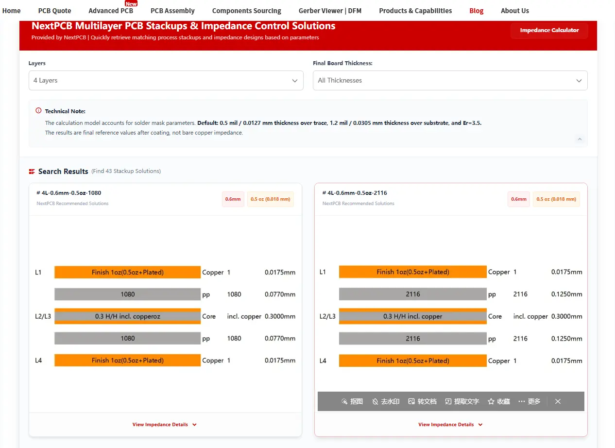
- Layer Count Coverage: The system includes all standard and advanced stack-up options ranging from 4 to 20 layers.
- Manufacturing Capability Matching: The impedance designs and stack-up solutions provided on the page fall within NextPCB's current recommended processes and manufacturing limits. Referencing this data helps reduce design changes caused by exceeding factory process constraints.
- Continuous Update Mechanism: It is important to note that the data in this system is updated periodically as NextPCB enhances its factory manufacturing capabilities and equipment, ensuring that engineers always have access to the latest, production-ready manufacturing parameters.
2. Data Benchmark Specifications: Accounting for Solder Mask Parameters
When calculating the impedance of a finished PCB, the solder mask (LPI) has a practical impact on the final results. This query system incorporates this factor into its calculation models. Specific parameter descriptions are as follows:
- Solder Mask Impact Included: The calculation models are not based on "bare copper" impedance in an ideal state but cover the dielectric influence after the solder mask is applied.
- Default Parameter Settings: Theoretical calculations on the page are based on the following standard production environment: Solder mask thickness over the trace is 0.5 mil, solder mask thickness over the substrate is 1.2 mil, and the solder mask dielectric constant (Er) is set to 3.5.
- Provision of Final Reference Values: The impedance values output in the query results are all final reference values after solder mask coating. This data more closely reflects the physical performance of the actual finished board, allowing engineers to reference it directly during simulation and design phases.
| Try NextPCB's Online Impedance Calculator |
Input your trace width, dielectric thickness, and Er value to instantly calculate characteristic impedance for microstrip and stripline structures — then lock in your stackup directly for manufacturing.
3. How to Use the Query System?
The system's operational logic is straightforward. Engineers can obtain the required data through the following steps:
- Select Layer Count (Layers): At the top of the page, click the corresponding number of layers (e.g., 4 Layers, 6 Layers, etc.) based on the project requirements. Once a specific layer count is selected, the system will automatically and immediately display all available stack-up solutions for that layer count below.
- Select Board Thickness (Final Board Thickness): Choose the desired finished board thickness (e.g., 0.8mm, 1.2mm, 1.6mm, etc.) from the secondary menu. After selecting a specific thickness, the system will filter the current results to further refine and display specific solutions that meet that thickness criteria.
- View Detailed Parameters: Upon completion of the filtering, the page will output the corresponding PCB Stack-up Diagram and a detailed impedance parameter table. The data dimensions include: Layer Type, Target Impedance (Single-ended/Differential), Width, Spacing, and Reference Plane.
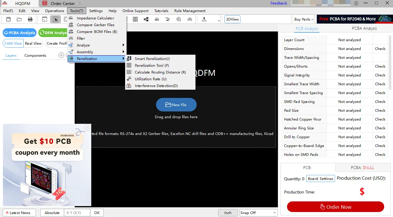
4. Data Source and Advanced Tools: HQDFM Desktop Edition
The stack-up and impedance data in the aforementioned web-based query system are all derived from and powered by the "Impedance Calculator", a built-in tool within the HQDFM Desktop Edition client.
If your design involves non-standard or special stack-up requirements, or if you require a comprehensive DFM (Design for Manufacturability) analysis, it is recommended to use the desktop software for more complete support: Download HQDFM Desktop Edition.
Appendix: Overview of HQDFM Desktop Edition Core Tool Suite
HQDFM is an integrated platform for PCB design and DFM analysis. Beyond impedance calculation, its built-in tool suite covers multiple stages of PCB production verification:
1. Core Design Verification Tools
- Impedance Calculator: Precisely calculates PCB impedance parameters to assist in high-speed signal design.
- Compare Gerber / BOM: Automatically compares different versions of Gerber files and BOM lists to locate design discrepancies or missing components.
- Filter: A data filtering tool used to isolate and review critical design information.
2. Advanced Design Analysis Tools
- Compare IPC Nets: Verifies network topology according to IPC industry standards to check for regulatory compliance.
- Calculate Copper Area / Net Length: Measures copper coverage area and trace lengths to assist in thermal design and routing timing evaluation.
- Test Point Analysis: Automatically analyzes test point layouts to evaluate testing coverage for production and assembly.
3. PCBA and Component Management Tools
- Count Solder Pads & Component Search: Automatically counts solder pads and retrieves components to assist in assembly cost estimation and design review.
- Export Centroid Data & Polarity Confirmation: Exports component coordinate data required for SMT and scans for polarity errors (e.g., reversed diodes or capacitors) to prevent assembly accidents.
4. Panelization and Production Optimization Tools
- Smart & Manual Panelization: Provides AI-assisted automatic panelization and highly customizable manual panelization functions to optimize material utilization.
- Utilization Rate & Interference Detection: Calculates material utilization rates and detects mechanical and electrical interference issues within the panel layout.
Summary: The NextPCB Impedance Control and Stack-up Query System provides an online stack-up reference manual that incorporates actual solder mask parameters, helping engineers plan impedance solutions that align with factory processes in the early design stages. For projects requiring complex structures or comprehensive DFM checks, it can be combined with HQDFM Desktop Edition for systematic design verification.
Ready to Manufacture Your Impedance-Controlled PCB?
NextPCB supports ±10% impedance tolerance with full stackup confirmation before production. Submit your Gerber files and stackup requirements to get a quote within 24 hours.

 NextPCB Capabilities
 PCB Assembly
 Layer Buildup
 SMD-Stencils
 PCB Design-Aid & Layout
 Mechanics
 Quality
 Drills & Throughplating
 Factory & Certificate
 PCB Assembly Factory Show
Certificate
PCB Assembly Factory Show
Certificate


 Surface

