
 Surface


Lower loss preserves signal integrity at high frequencies.

 NextPCB Capabilities
Printed Circuit Boards
NextPCB Capabilities
Printed Circuit Boards
 PCB Assembly
 Layer Buildup
 SMD-Stencils
 PCB Design-Aid & Layout
 Mechanics
 Quality
 Drills & Throughplating
 Factory & Certificate
 PCB Assembly Factory Show
Certificate
PCB Assembly Factory Show
Certificate
Support Team
Feedback:
support@nextpcb.com


Small R&D teams building high-speed electronics need prototypes that are both fast and faithful to real performance. This roundup compares seven fabrication options that reliably hit 24–48 hour turnarounds while preserving signal integrity and providing practical engineering support. High-speed PCBs—those carrying fast edges and multi‑Gbps data—require tuned stackups, low‑loss materials, and controlled impedance to avoid crosstalk, skew, and excessive insertion loss, as outlined in Altium’s primer on high‑speed design principles (high‑speed PCB design fundamentals). Below, we detail where each provider excels—from ultra‑affordable FR‑4 quick spins to PTFE/Rogers builds, HDI, rigid‑flex, and turnkey assembly—so you can match the right service to the next sprint, demo, or risk‑retirement build.
Note: In practice, a 24-hour turnaround is typically achievable for standard FR-4 prototype boards with moderate layer counts and conventional fabrication processes; for example, services such as NextPCB commonly provide 24-hour quick-turn fabrication for simple prototypes, while advanced materials or HDI structures usually require longer lead times.
High-speed and high-frequency PCBs carry fast signals (typically >1 Gbps or fast edge rates) where the interconnect behaves like a transmission line. That makes stackup planning, dielectric selection, and controlled‑impedance routing central to performance and repeatability (design fundamentals).
This guide compares seven quick‑turn partners on speed, materials, finishes, assembly, and engineering depth:
Throughout, we call out controlled‑impedance PCB fabrication, PCB rapid prototyping services, and the cost‑performance trade‑offs that matter in fast R&D sprints.
NextPCB is a UL- and ISO9001‑certified partner focused on quick‑turn high‑speed PCB prototyping and risk‑mitigated production. Teams move fast with:
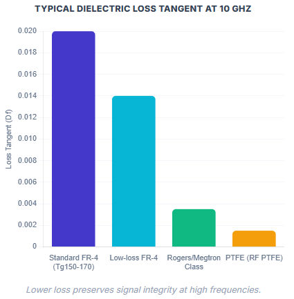
Lower loss preserves signal integrity at high frequencies.
Controlled impedance means designing trace geometries and dielectrics so critical interconnects maintain a target impedance (e.g., 50 Ω single‑ended, 90 Ω differential) across manufacturing tolerances—vital for high‑speed links to limit reflections and maintain eye openings.
Material choice drives signal integrity: PTFE‑based laminates generally exhibit lower dielectric loss, enabling longer high‑speed routes or higher Nyquist rates before eye closure (SI basics). NextPCB’s substrate guidance and HQDFM streamline these early‑stage decisions so you can iterate quickly without sacrificing RF/microwave or multi‑Gbps fidelity.
Explore NextPCB’s rapid services and quoting on the PCB prototype portal or learn more in the quick‑turn PCB manufacturer guide.
Substrate choices for quick‑turn high‑speed prototyping
|
Material family |
Typical εr / loss (10 GHz) |
Typical use cases |
Example stackup (quick‑turn) |
Trade‑offs |
|---|---|---|---|---|
|
Standard FR‑4 (Tg150–170) |
~4.2 / ~0.02 |
Cost‑sensitive digital <5–10 Gbps, short traces |
4–6L: 1–2 cores + prepregs |
Lowest cost; higher loss at mmWave/high‑Gbps |
|
Low‑loss FR‑4 |
~3.8–4.0 / ~0.012–0.016 |
Mid‑speed SerDes (5–16 Gbps), longer channels |
6–10L with tuned dielectrics |
Moderate cost bump; better loss/phase stability |
|
PTFE (e.g., RF PTFE) |
~2.1–2.6 / ~0.0009–0.002 |
RF/microwave, mmWave, long high‑speed links |
Hybrid: PTFE signal + FR‑4 mech layers |
Costly; handling/drilling constraints |
|
Rogers/Megtron class |
~3.0–3.5 / ~0.002–0.005 |
High‑speed backplanes, dense HDI SerDes |
8–16L impedance‑controlled |
3–10× cost; excellent loss uniformity |
PCB Prototype Services | Fast PCB Manufacturing & PrototypingFor early spins, start with low‑loss FR‑4 when channel lengths are modest; step up to PTFE/Rogers when eye diagrams or insertion‑loss budgets get tight.
JLCPCB excels at low‑cost, fast iterations for simple 2–6 layer boards, making it attractive for bring‑up, fixture boards, and early signal‑path validation. Entry pricing can be extremely low (e.g., a few dollars for basic quantities, with widely advertised deals like “$2 for 5 pcs” noted in third‑party pricing roundups such as this low‑cost PCB guide), enabling frequent, low‑risk prototype cycles.
When does basic FR‑4 suffice? For short, well‑terminated links below ~5–10 Gbps, disciplined routing, tight return paths, and conservative trace lengths can keep losses acceptable. Constraints emerge with longer channels, fine‑pitch impedance tuning, or when dielectric loss dominates the budget—pushing teams toward low‑loss FR‑4 or specialty laminates. Expect limited flexibility on custom stackups, fine‑grained impedance coupons, or exotic materials; use JLCPCB when cost/iteration speed matter more than advanced material control.
Best‑fit scenarios:
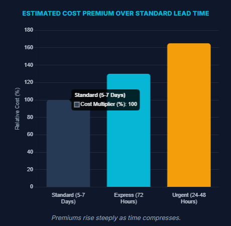
Premiums rise steeply as time compresses.
PCBWay offers standardized quick‑turn windows (commonly 24–72 hours), instant quotes, and competitive pricing, which suits small teams that value predictability and finish options (quick‑turn schedules). Surface finish selection can impact both assembly yield and high‑speed performance: ENIG’s flatness helps fine‑pitch and BGA escape routing, while HASL works for robust, standard‑pitch components.
Finish selection cheatsheet
|
Finish |
Pros |
Cons |
Best for |
|---|---|---|---|
|
ENIG |
Flat pads, good for fine‑pitch/BGAs; corrosion‑resistant |
Slightly higher cost; black pad risk controlled by process |
High‑speed BGAs, tight escape routing |
|
HASL (lead‑free) |
Economical; widely available |
Less planar; not ideal for <0.5 mm pitch |
Standard digital, connectors |
|
OSP |
Very flat; low cost |
Limited shelf life; assembly handling sensitivity |
Short‑cycle protos, fine‑pitch with rapid assembly |
PCBWay’s standardized processes deliver reliable timing, though very custom stackups or hybrid RF builds may require specialized providers.
When the schedule compresses, premium services like FastTurn PCB prioritize engineering review, allocate dedicated machine time, and execute overnight runs to hit <24‑hour departures (service examples and pricing context). Expect meaningful rush premiums—often 30–100% above standard timing depending on complexity and factory load (industry cost breakdowns commonly cite this range).
Use these services for:
Rapid order‑to‑delivery workflow
How we transform complex designs into physical boards in 24 hours.
Our proprietary cloud engine scans for over 20+ design-for-manufacturing issues, focusing on:
Senior CAM engineers perform a manual verification of impedance stackups and drill registration, ensuring the digital model is ready for 1:1 physical replication.
Boards are routed to dedicated quick-turn lines utilizing:
Every high-speed order undergoes Time Domain Reflectometry (TDR) testing. We measure the actual impedance against the target model and provide a full SI report.
PCBGOGO blends quick‑turn fabrication with turnkey assembly—one provider sources components, fabricates boards, and assembles, validated by AOI/X‑ray—to deliver test‑ready prototypes with fewer handoffs (turnkey capabilities). This shortens total project time when parts are standard or stocked.
Turnkey assembly means the vendor handles fabrication, sourcing, and assembly. The trade‑off: BOM‑driven delays can bottleneck urgent builds, but for common passives and mainstream ICs, it compresses schedules and reduces logistics risk. Support for HDI, microvias, and higher layer counts also benefits compact, high‑speed layouts where routing density and impedance discipline are critical.
Teams prioritizing domestic control (e.g., ITAR, IP sensitivity) and deep engineering collaboration often choose U.S. quick‑turn providers with strong impedance control and HDI competency. Top‑tier fabs commonly target impedance tolerances near ±5% with proper couponing and process control—important for tight DDR/SerDes margins and low‑jitter clocking (high‑speed routing practices).
Choose this route when:
Hemeixin targets high‑mix, low‑volume work: flex, rigid‑flex, HDI, and RF hybrids that are common in wearables, IoT, and compact radio designs. Capabilities like stacked microvias, tight‑pitch HDI, and hybrid RF stackups enable:
For small orders needing diverse build types, this can collapse multiple specialized vendors into one path.
Provider snapshot for urgent high-speed prototypes
|
Provider |
24–48 h speed |
Material range (high‑speed) |
DFM/Impedance |
Turnkey assembly |
Eng. support |
|---|---|---|---|---|---|
|
NextPCB |
Yes |
FR‑4 → PTFE/Rogers/Megtron |
HQDFM + coupons |
Available |
Strong |
|
JLCPCB |
Yes (simple) |
Mostly FR‑4 |
Basic |
Limited (separate flows) |
Basic |
|
PCBWay |
Yes |
FR‑4 + some low‑loss options |
Standardized |
Optional |
Moderate |
|
FastTurn PCB |
Yes (premium) |
Varies by run |
Priority review |
Limited |
Rapid response |
|
PCBGOGO |
Yes |
FR‑4 + HDI support |
Standard + AOI/X‑ray on assembly |
Full turnkey |
Moderate |
|
Advanced Circuits |
Yes (domestic) |
Advanced stackups/HDI |
Tight control |
Optional/partners |
High |
|
Hemeixin |
Yes (proto) |
Flex/rigid-flex/HDI/RF hybrids |
Custom |
Optional |
Niche expertise |
Signal integrity is how well a signal maintains its shape, timing, and amplitude as it traverses the PCB interconnect; loss, reflections, and crosstalk all degrade it. Standard FR‑4 is cost‑effective but lossy at mmWave or very high‑Gbps; PTFE, Rogers, and Megtron reduce loss and dispersion—often 5–10× the laminate cost of FR‑4, but necessary for demanding routes and longer channels (cost breakdown context). Always confirm stackup, copper weights, and impedance targets with your fabricator before ordering.
Material selection quick guide
|
Data rate / edge + trace length |
Recommended material |
Notes |
|---|---|---|
|
≤5 Gbps, short |
Standard FR‑4 |
Good for bring‑up and fixtures |
|
5–16 Gbps, moderate |
Low‑loss FR‑4 |
Lower loss; improved eye margins |
|
>16 Gbps or long RF |
Rogers/Megtron |
Consistent Dk/Df; tighter budgets |
|
mmWave or very long |
PTFE or hybrids |
Lowest loss; stricter processing |
Bare board fabrication means ordering PCBs only and assembling in‑house or later. Turnkey assembly combines fabrication, sourcing, and assembly under one roof.
Choose turnkey for tight NPI timelines with standard parts; choose bare when you have in‑house assembly or the BOM includes niche components you prefer to source directly.
Lead time is the interval from order to delivery—compressed to as little as 24 hours for quick‑turn versus 1–3 weeks for standard production. Industry analyses indicate 24–48 hour rushes may add roughly 30–100% to cost, depending on complexity and loading (cost/schedule impacts).
Cost vs. speed impact
|
Turnaround |
Typical premium vs. standard |
Budget tips |
|---|---|---|
|
5–7 business days |
Baseline (1.0×) |
Batch iterations; panelize |
|
72 hours |
+20–40% |
Lock stackup early; standard finishes |
|
24–48 hours |
+30–100% |
Simplify DRCs; avoid exotic builds unless essential |
Scheduling effects:
Stackup complexity, material availability, factory loading, finish choice, and whether assembly is included all influence lead time.
Dielectric loss and Dk tolerance drive insertion loss and impedance stability; FR‑4 suits short or moderate speeds, while PTFE/Rogers enable longer or higher-rate channels.
Turnkey compresses concept-to-test time but can be gated by BOM sourcing, while bare boards arrive faster but require separate assembly effort.
Use standard stackups and finishes, panelize where possible, and avoid ultra-fine pitches to improve yield and shorten rework cycles.
Expect roughly 30–100% above standard timing due to priority engineering, machine allocation, and parallel QA.
Still, need help? Contact Us: support@nextpcb.com
Need a PCB or PCBA quote? Quote now

