Choosing between a local European manufacturer and NextPCB is less about simple "labor costs" and more about balancing administrative friction, risk mitigation, and component procurement ecology across your project’s lifecycle.
1. The European Advantage (Zero Friction & Compliance)
For European hardware teams, local manufacturers (such as Eurocircuits or Aisler) are unparalleled when peace of mind and regional regulations are the top priorities.
- Zero Administrative Friction: Buying locally eliminates the "customs roulette." You get next-day local delivery, seamless domestic VAT billing, and zero import compliance hurdles.
- Strict Regulatory & Data Sovereignty: Local fabs ensure total compliance with strict EU data privacy (GDPR), medical, and defense mandates. Your intellectual property (IP) stays legally protected within EU borders, making them essential for ITAR/military-restricted or state-regulated projects.
- The Sourcing Bottleneck (Con): Local European fabs rarely carry native component stock. They source your BOM on-demand from Western catalog distributors (Mouser, DigiKey, Farnell), forcing you to pay premium retail markup prices and exposing your project to local parts shortages.
2. The NextPCB Advantage (Turnkey Ecosystem & Seamless Scaling)
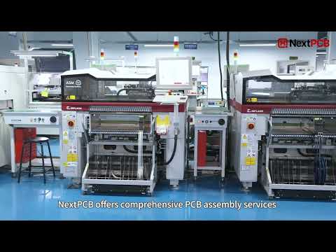
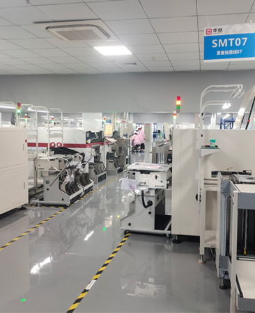
NextPCB bridges the gap between affordable prototyping and high-volume, industrial-grade manufacturing by leveraging Asia’s massive component ecosystem.
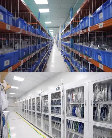
- Turnkey Sourcing Ecosystem: NextPCB eliminates the "component hunting" headache. Backed by our native HQ Online marketplace with 600,000+ in-stock parts, they bypass Western retail distribution, secure massive volume discounts, and handle fabrication, sourcing, and assembly under one roof.
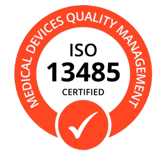
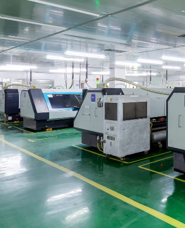
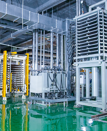
- Industrial-Grade Capacity & Certifications: They don't just offer lower prices; they deliver certified reliability. Operating under IATF 16949 (Automotive) and ISO 13485 (Medical) standards, NextPCB allows you to transition seamlessly from a 1-piece prototype to millions of units without changing vendors.
- Import Variables (Con): Orders are subject to international transit (3–5 days via Express), require navigating EU import customs/VAT paperwork, and involve a 6-hour time-zone gap for back-and-forth engineering revisions.
3. The Recommended Hybrid Strategy
Most successful European hardware teams use a split pipeline: Use local European fabs for emergency 48-hour bare-board bench tests or compliance-restricted R&D. Then, shift to NextPCB for beta runs and mass production to maximize your profit margins and leverage their direct-manufacturer parts sourcing.


 24 hours Quick-turn Prototype
 Scale Production
 PCB Assembly - Fast As 7 Days Prototype
 Components Sourcing
 Online Gerber Viewer
 Free DFM Software