
 NextPCB Capabilities
Printed Circuit Boards
NextPCB Capabilities
Printed Circuit Boards
 PCB Assembly
 Layer Buildup
 SMD-Stencils
 PCB Design-Aid & Layout
 Mechanics
 Quality
 Drills & Throughplating
 Factory & Certificate
 PCB Assembly Factory Show
Certificate
PCB Assembly Factory Show
Certificate
Support Team
Feedback:
support@nextpcb.com


A solder ball is a glob of solder that connects a PCB and chip package. In multichip panels, you can also link stacked boxes using solder boards.
They can be manually or automatically installed on circuit boards using various tools. Often, a sticky flux is for the ensure their location. Moreover, the most frequent flaw that hinders SMT assembly procedures is solder balls.
Solder balls have two disadvantages, though. A solder ball that is broader than 0.13mm in diameter or placed close to traces infringes on the minimum electrical clearance rule.
Several mistakes can result in a solder ball that results in flaws in a constructed PCB.
As long as they undergo proper storing, solder balls do not produce faults, according to IPC. The good, the bad, and the ugly of solder balls are examined in this essay.
Due to their geometry, solder balls are also possible to name solder bumps or solder spheres. A spherical piece of solder, a solder ball, is used to join chip packages to PCBs.
Via consecutive flow/quench or reflow procedures, solder balls are produced. These procedures are followed by their degreasing and classification.
By flattening a solder ball's ball shape into a coin shape, you can improve contact reliability. A coin Solder ball is a name for such an incident.
A solder ball might potentially result in Board flaws. These may jeopardize a PCB electronic's electrical dependability. Solder balls that are 0.13 mm or larger in diameter than traces violate the minimum electrical clearance rule.
According to the IPC A 610 standard, even solder boards with a diameter of less than 0.13mm might have flaws.
Five solder balls with the required diameter are inserted with a gap of 100mm2, which causes these flaws. Both automated reflow and hand soldering might unintentionally produce harmful solder balls. The solder ball creates a problem when it is not twisted in the conformal coating or the no-clean residue.
However, determining whether the ball got caught in a conformal coating or a no-clean residue could be challenging. Nonetheless, brush sweeping is a simple and trustworthy method you can apply to find out.
It won't result in flaws if it stays put after you brush them with a brush. That is the IPC's position on the situation. There are several methods for troubleshooting a bad solder ball. The best way for debugging starts by trying to locate the point where the undesired solder ball appears. The faulty solder ball can appear during the pick-and-place procedure, reflow, or printing process.
The majority of consumer electronics contain solder balls as essential components. Getting solder boards right has become more crucial as consumers want smarter, more powerful, and more portable gadgets. Nevertheless, solder balls are still among electrical circuitry's most intricate and sensitive parts. Its use necessitates a high level of diligence.
A solder ball valve is the best way to connect several chip stacks on a PCB. It has the ability to control how signals and electrons move among the pile's numerous layers.
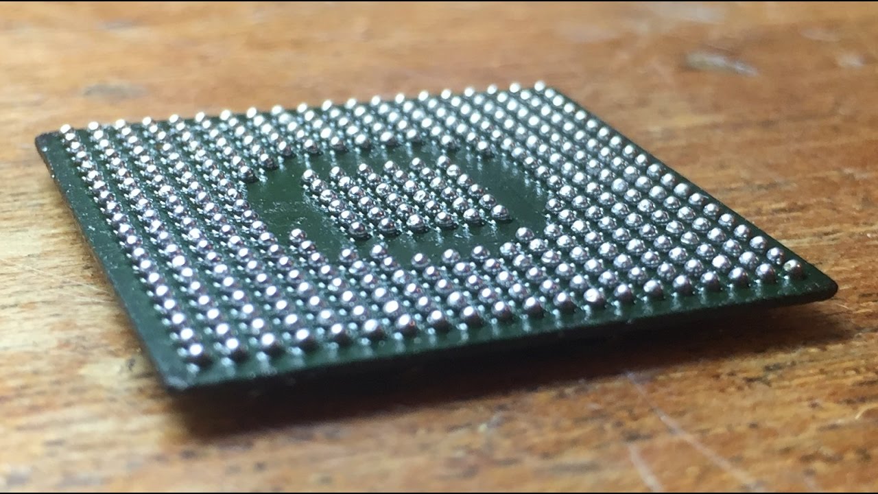
A Ball Grid Array often houses solder ball valves (BGA). A dual in-line or flat package often has less interconnectivity than a BGA.
The process outlined here involves utilizing a ball pickup tool to solder ball valves onto BGA packages.
The main goal is to arrange solder balls in a grid on a substrate. The conductive locations on other substrates are possible to connect using this substrate.
You'll need a ball pick-up gadget to use this technique. Using vacuum suction, this ball pickup device pulls solder balls out of a fluidized ball reservoir. That suggests that you require a reservoir for solder balls that holds a number of ready-made solder balls. Moreover, the reservoir must contain adhesives. You obviously need at least one vacuum, according to it.
That also implies that you require at least one vacuum source in order to provide suction to the tool's opening.
A prefabricated solder tool is possible to insert into at least one opening on the vacuum suction tool.
Moreover, it has a controlled ball seat coupled to two sources of vacuum and pressure. The instrument uses a jet of gas to inject the selected solder balls into the substrate's conductive locations. The substrate pads are put in a reservoir with fluidized balls in a different technological setup. A flux or adhesive that draws and binds with the solder balls in the pool is used to apply the coating.
The 3-Orifice design is one of the oldest and most popular ways to make solder balls.
In this procedure, you must first obtain a solid solder alloy, preferably an Sn63Pb37 or a lead-free solder. Create a solder sheet or a solder wire using the solder alloy. For a wire, cut the wire into tiny pieces, and for a solder sheet, scratch out specks.
Measure out the parts and pieces so that they will precisely generate the volume of a solder ball that is 2mm in diameter. The bits and specks should then be added to a column of heated oil to melt. The hot crude column's upper portion ought to be warmer than the melting point.
Also, the temperature in the lower part should be below the melting point.
When the fragments and specks in the column of hot oil melt, you'll have the solder balls you want. In a viscous liquid, chill the balls after that.
Be aware that the presence of oxides in the column may distort the spherical shape of the balls. To avoid this, you can cover the column with a flux film. This approach is both inexpensive and quite effective. With this technique per second, you may produce up to 7,000 high-quality solder balls in any orifice. Yet, there are drawbacks to the method as well. To begin with, the method may end up messy and prone to contamination.
The weight of each ball will vary, but you may measure their values. Also, it is very difficult to find balls with a 1.5% tolerance. The Value of Packing for Forming Solder Balls As mentioned above, the presence of oxides can cause the solder ball's form to change. Packaging is one method of preventing the oxidation of the solder balls.
Packaging can not only keep oxygen from being removed, but it can also extend the shelf life of the solder balls even after their expiration date.
Your solder paste's moisture content may contribute to solder balls blowing up during reflow. During cooling, water penetrates the solder paste.
The paste will absorb moisture if it is not allowed to come to room temperature after being taken out of the refrigerator. But baking will get rid of the water.
While hand soldering, the board itself may produce unwanted solder balls. Unwanted solder balls may result from cleaning the board with alcohol, air, or moisture.
These pollutants can enter a board with damaged or missing plating through holes, open vias, and between layers. Also, these pollutants get pushed out of the board during the reflow process when they get subjected to heating.
Their rapid exit sends gases flying in all directions, which causes liquid solder to blow on everywhere. As paste flux gases escape from the panel portions near the surface, they could likewise have a similar effect.
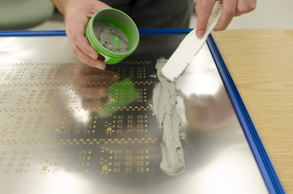
It's possible that your stencil is selectively laying solder paste. You must make sure your under-stencil cleaning procedure is effective and comprehensive.
It's possible that you're using an improper, overly thick under-stencil wiping roll. The balls may extend across the underside of the stencil if the registration is not thick enough. Also, the excess balls end up on the PCB when the stencil is subsequently undergoing the process.
Poorly designed solder pastes may blast liquid solders in all directions when heated and reflowed.
The most likely reason for the explosion is typically the volatile ingredients.
Explosions like this are possible to avoid by lowering the preheat ramp rate in these circumstances. This makes it possible to expel the volatile substance gradually rather than suddenly. However, you must make sure to warm it gently enough.
There are many undergoing research studies to demonstrate how the Pd film thickness affects the dependability of solder ball joints.
Electroless Ni/Pd/Au plating on an Sn-3.0Ag-0.5Cu (SAC305) solder ball joint was the focus of the survey. Solder ball shear testing is for the investigation.
The Pd film thickness between 0.05 and 0.02 microns was ideal for reliable solder joints after several reflow cycles.
Tests have also demonstrated that 0.02-micron thick electrodes are more dependable for solder ball joints. This outcome surpasses that of electroless Ni/Au plating even more. The study also demonstrates that the dependability of a solder ball depends on the form and thickness of the intermetallic compounds (IMCs).
The dependability of a solder ball was significantly impacted by the degree of adhesion at the dendritic layer of the IMCs/solder contact. Moreover, it was demonstrated that (Cu, Ni, Pd)6Sn5 IMCs with minute Pd give outstanding solder ball joint reliability, mostly as a result of Pd preventing IMC growth.
Defective solder boards can occur for a number of reasons. Below is a list of some of the most typical causes:
1. Verify that the dimensions and compatibility of the mat and template are accurate.
2. As soon as possible, properly clean the stencils.
3. Modify the printing pressure for the solder paste.
4. Closing the space between the stencil and PCB.
5. Applying an additional solder mask in between the pads.
6. Modify the pressure before picking up and putting the nozzle.
7. Separating the new and old flex.
Solder balls lead to some advantageous conditions and some disadvantageous conditions. Ball Grid Array is one of the most common advantageous purposes of the solder ball, while the solder ball that developed in the soldering process makes a bad impact on the PCB design. There are several factors that lead to the solder ball developing while hand soldering. That could be due to moisture, PCB design issues, and issues in the soldering process.
Most Solder ball issues are possible to minimize practicing the right way of soldering and inspecting the solder ball defects correctly. If you cannot minimize the Solder Ball issue, getting help from industry experts is better.
Still, need help? Contact Us: support@nextpcb.com
Need a PCB or PCBA quote? Quote now


 Surface

