NextPCB Capabilities
 PCB Assembly
 Layer Buildup
 SMD-Stencils
 PCB Design-Aid & Layout
 Mechanics
 Quality
 Drills & Throughplating
 Factory & Certificate





Grid Copper vs. Solid Copper Pour: Choosing the Right Copper Fill for Your PCB
By NextPCB Engineering Team | Last updated: August 2026 | Reading time: 5 min
Copper pour (also called copper fill or copper flood) is used across large open areas of a PCB — typically for ground or power planes — to reduce impedance, improve heat dissipation, and provide EMI shielding. When designing a copper pour, engineers generally choose between two fill styles: grid (hatched/mesh) copper and solid copper. The right choice depends on the circuit's frequency, current requirements, and how the board will be manufactured and assembled.
Grid Copper: Best for High-Frequency, Anti-Interference Designs
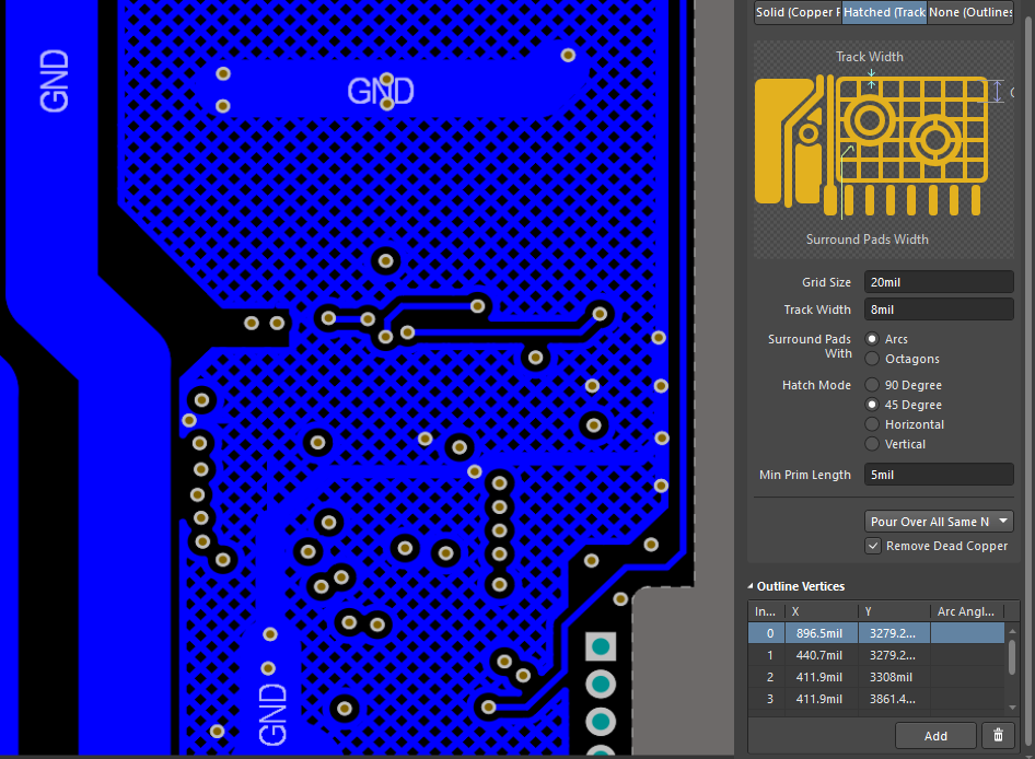
Grid copper — also known as hatched or cross-hatched copper — fills a region with a mesh pattern of intersecting copper traces rather than a single continuous plane. This style is generally preferred for high-frequency circuits where EMI shielding and interference suppression are priorities, since the segmented copper pattern still provides an effective reference and shielding surface for high-frequency signals while behaving differently from a solid plane in terms of thermal stress distribution.
A key manufacturing advantage of grid copper is thermal: large solid copper areas absorb and retain heat unevenly during the wave soldering stage of SMT assembly, and the mismatch in thermal expansion between a large solid copper region and the surrounding laminate can cause the board to warp or bow. Because grid copper has less continuous copper mass and more resin exposed within the mesh openings, it distributes thermal stress more evenly across the panel and reduces the risk of warping during wave soldering — an important consideration for boards with large ground or shield areas that will pass through a wave solder process.
Solid Copper: Best for Low-Frequency, High-Current Designs
Solid copper pour, by contrast, is the preferred choice for low-frequency circuits carrying large currents, such as power supply planes, motor drive boards, or high-current power distribution layers. A continuous copper plane has lower DC resistance and greater current-carrying capacity than an equivalent-area grid pattern, since the mesh openings in grid copper effectively reduce the cross-sectional area available for current flow. For power and ground planes where minimizing IR drop and heat buildup from resistive losses matters more than high-frequency shielding behavior, solid copper is the more reliable option.
Recommended Design Rules for Grid Copper
When laying out a grid (hatched) copper pour, the following minimum dimensions are recommended to maintain reliable etching, adequate current capacity, and manufacturing consistency:
- Line (trace) width: ≥ 8 mil (0.2 mm)
- Line spacing (gap between grid lines): ≥ 8 mil (0.2 mm)
Grid lines narrower than this threshold increase the risk of open circuits from over-etching during fabrication, particularly on panels with variable copper thickness. Spacing tighter than 8 mil also raises the risk of solder mask bridging and makes the pour more difficult to inspect reliably during AOI. These values are a practical starting baseline — designers working with heavier copper weights (2oz and above) or very high-current nets should widen both the line width and spacing beyond these minimums and confirm current-carrying capacity against IPC-2152 trace current tables for the specific copper weight in use.
Summary
Choosing between grid and solid copper pour comes down to a trade-off between EMI performance/thermal stability and raw current-carrying capacity. Grid copper is generally the better fit for high-frequency, interference-sensitive designs and boards going through wave soldering, while solid copper remains the standard choice for low-frequency, high-current power and ground planes. When using grid copper, keeping line width and spacing at 8 mil or greater helps ensure a reliable, manufacturable result.