NextPCB Capabilities
 PCB Assembly
 Layer Buildup
 SMD-Stencils
 PCB Design-Aid & Layout
 Mechanics
 Quality
 Drills & Throughplating
 Factory & Certificate





PCB Design Considerations: 5 Key Rules for Signal Integrity and Reliable Manufacturing
By NextPCB Engineering Team | Last updated: August 2026 | Reading time: 8 min
PCB design is the foundation that determines the performance, manufacturability, and reliability of every printed circuit board that follows it. A layout mistake made at the design stage — an unmatched trace impedance, a poorly routed differential pair, an unsuitable board material — is far more expensive to fix after fabrication or assembly than during layout. Based on common issues we see in customer Gerber files during DFM review, this guide summarizes five design considerations engineers should evaluate before sending a board to production, with practical guidance drawn from IPC design standards and everyday manufacturing feedback.
1. Choosing the Right PCB Board Material
Selecting a substrate is always a balance between electrical performance, mechanical requirements, manufacturability at volume, and cost. On the electrical side, key parameters include the dielectric constant (Dk), dissipation factor (Df), and how stable these values remain across frequency and temperature. On the mechanical side, factors such as the glass transition temperature (Tg), thermal expansion coefficient (CTE), and thickness tolerance affect how the board survives assembly reflow and long-term thermal cycling.
Standard FR-4 laminate is adequate for the majority of digital and low-frequency analog designs and remains the most cost-effective, widely available option for volume production. However, material selection becomes far more critical once signal frequencies climb into the GHz range, which is common in RF modules, 5G infrastructure, radar, and high-speed serial links (e.g., PCIe Gen4/5, 100G+ Ethernet). At these frequencies, FR-4's higher and less stable Df leads to significant dielectric loss, and standard weave glass styles can introduce fiber-weave-related skew between differential pairs.
For these applications, low-loss materials such as Rogers RO4000-series, PTFE-based laminates, or hybrid stack-ups (Rogers core with FR-4 outer layers to control cost) are typically specified. IPC-4101, the standard specification for base materials used in rigid and multilayer boards, is a useful reference when comparing datasheet parameters across suppliers. The right choice ultimately depends on the highest signal frequency on the board, the length of critical traces, and the production volume — material selection made in isolation from these factors is one of the most common sources of downstream signal integrity failures.
2. Avoiding High-Frequency Interference (Crosstalk)
Crosstalk is unwanted coupling of energy from one signal trace to another through electromagnetic fields, and it becomes more pronounced as edge rates and clock frequencies increase. The basic strategy for controlling crosstalk is to minimize the coupling path between aggressor and victim traces — primarily by increasing physical separation and reducing the length over which two traces run parallel.
A widely used rule of thumb in the industry is the "3W rule": maintaining a spacing of at least three times the trace width (measured center-to-center) between adjacent parallel traces reduces coupled crosstalk to roughly 70% or less of what it would be at minimum spacing. Additional practical measures include:
- Routing high-speed digital traces and sensitive analog traces on separate layers, ideally with a solid ground plane between them
- Avoiding long parallel runs — routing traces at right angles where they must cross layers reduces coupling length
- Using guard traces or ground stitching vias around especially sensitive nets, such as clock lines or ADC inputs
- Keeping a continuous, unbroken reference plane beneath high-speed traces to control the return current path
These techniques are especially important where high-speed digital buses run near low-level analog or RF circuitry, since coupled noise in that scenario can directly degrade measurement accuracy or receiver sensitivity.
3. Solving Signal Integrity Issues
Signal integrity problems are, at their core, impedance mismatch problems. When a signal traveling down a trace encounters a change in impedance — at a connector, a via, a branch point, or the receiving device itself — part of the signal energy reflects back toward the source instead of continuing to the load. These reflections cause overshoot, undershoot, ringing, and, in severe cases, logic-level errors or EMI.
Four factors primarily determine whether impedance stays matched along a signal path:
- Source impedance — the output impedance of the driving device
- Trace characteristic impedance — determined by trace width, copper thickness, dielectric height, and dielectric constant of the material beneath it
- Load characteristics — the input impedance and capacitance of the receiving device
- Routing topology — how the trace branches to reach one or multiple loads (point-to-point, daisy chain, star, or fly-by)
The two primary tools for resolving impedance mismatches are termination and topology adjustment. Series termination (a resistor placed near the driver) is common for point-to-point single-load nets, while parallel or Thevenin termination near the receiver is more common on buses with multiple loads or longer trace runs. Choosing the correct topology — for example, a fly-by topology with individually terminated stubs for DDR memory buses — is often just as important as the termination method itself. Controlled-impedance routing should be verified against a stack-up impedance calculation (or a field solver) rather than assumed from trace width alone, since actual impedance depends on the full cross-section of the trace and adjacent copper.
4. Implementing Differential Pair Routing
Differential signaling is used extensively in modern high-speed interfaces — USB, HDMI, Ethernet, PCIe, and LVDS — because it offers strong noise immunity and reduced EMI compared to single-ended signaling. Correct layout of a differential pair depends on two main rules:
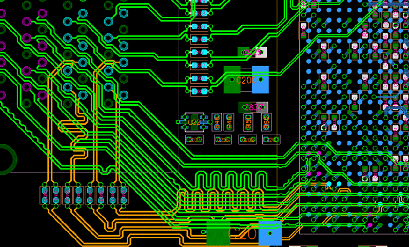
- Length matching: the two traces of a pair should be as close to equal length as possible. Mismatch introduces skew, which degrades the common-mode rejection that makes differential signaling effective in the first place. Small length differences are typically corrected using controlled serpentine (accordion) tuning placed close to the source of the mismatch, such as near a connector or via transition.
- Constant spacing: the gap between the two traces should remain uniform along the entire route, since this spacing — together with trace width and dielectric height — determines the differential impedance (commonly 90Ω or 100Ω depending on the interface standard). Any necking or spreading of the pair, even briefly to route around an obstacle, creates a local impedance discontinuity.
Differential pairs can be routed in two configurations: side-by-side, where both traces run on the same layer with a fixed gap between them, or over-under, where the two traces run on adjacent layers separated by the dielectric, stacked directly on top of one another. Side-by-side is more common and easier to control for impedance and length matching; over-under is sometimes used where routing density on a single layer is constrained, but it is more sensitive to layer-to-layer registration during fabrication and is generally more difficult to hold to a tight impedance tolerance.
5. Single-Ended Clock Signal Lines
Not every clock or timing signal uses differential signaling. When a clock line has a single-ended driver and a single-ended receiver — meaning neither the source nor the load is a differential I/O — differential routing techniques (paired traces, controlled differential spacing) do not apply, because there is no complementary signal to pair it with.
In this case, the line should instead be treated as a standard single-ended controlled-impedance trace, typically targeting a characteristic impedance such as 50Ω, with routing practices that still apply from the sections above: a continuous reference plane, appropriate spacing from adjacent traces to limit crosstalk (per the 3W guideline), and termination selected based on the driver's output impedance and the trace's electrical length relative to the clock's rise time. Applying differential-pair rules to a single-ended clock net is a common design error that adds unnecessary routing complexity without providing any actual signal integrity benefit.
Summary
These five considerations — material selection, crosstalk avoidance, signal integrity through impedance matching, differential pair routing, and correctly identifying single-ended versus differential nets — form the baseline for a manufacturable, electrically sound PCB design. As operating frequencies and data rates continue to climb across consumer, industrial, and communications applications, the margin for error in each of these areas continues to shrink, making disciplined layout practice and early DFM review increasingly important parts of the design cycle.
Have a design under review and want feedback on stack-up, impedance, or routing before fabrication? NextPCB's engineering team offers free DFM analysis on submitted Gerber files.