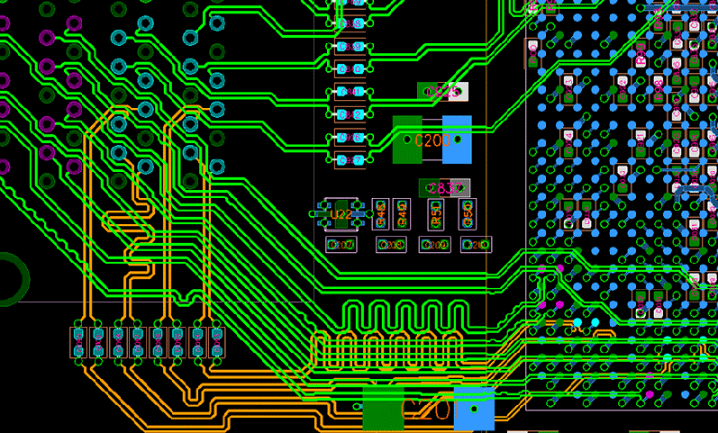
1.Questions about hole attributes
In this 3D drawing, the customer designs these 2 pads that need to be opened. However, these 2 holes are defined as VIA (via) attributes, and the customer select "via hole with solder mask" when placing the order. The two pads will be covered with the solder resist ink during manufacturing. Therefore, when processing this piece, please use PAD (component) attributes to design these holes and pads to avoid deviations during manufacturing.
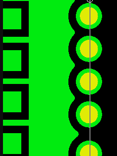
2.The hole spacing for half hole process
General half-hole design: The hole size and hole spacing should be above 0.5mm. There is only 0.45mm of the hole spacing in the following pic, which will lead to short-circuit. Therefore, pay attention to this detail when designing the half-hole, otherwise, it will cause unnecessary loss of the finished product. As shown:
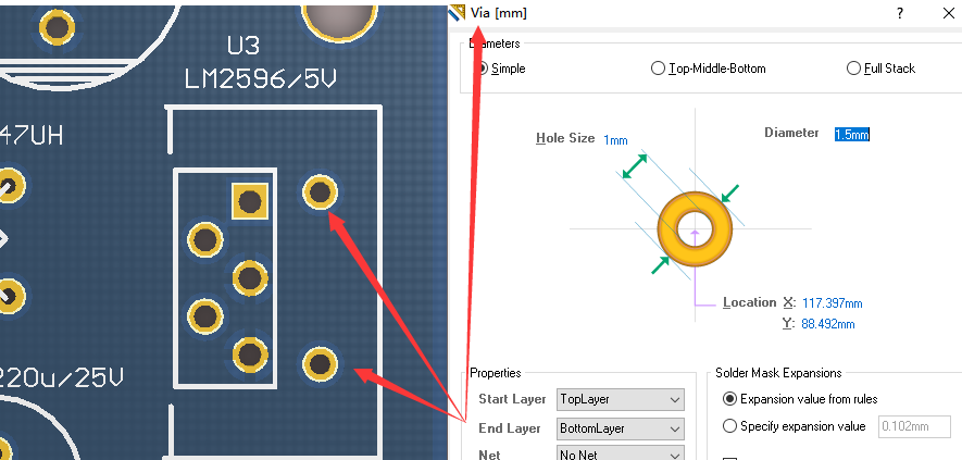
3.No pads in vias
In PCB design, the through-hole has a large inner diameter and outer diameter, and it is easy to produce without copper. Because the inner diameter is 0.6MM, it is recommended to reduce it to 0.3MM (the outer diameter remains unchanged). Same price, quality guaranteed.
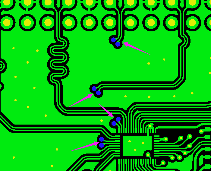
4.The optimal ratio of vias
In the case of sufficient space, the conventional via size 0.3mm-0.5mm is the optimal size. The outer diameter of the hole is 12mil larger than the inner diameter as the optimal ratio. For example, if the hole is 12mil, the outer diameter is 24mil, so that the inner and outer diameter ratio of the via (Via) is optimal. The outer diameter has a certain influence on the difficulty of production alignment and the reliability of the product. There are tolerances in each process of production. When the outer diameter ring is too small, the deviation of the drilling process and the line alignment process is too large. The final produced PCB will have the risk of blasting the ring (the board factory calls it a "broken pad"). When there is a broken pad, there is also a risk of insufficient current carrying for the product.

 NextPCB Capabilities
 PCB Assembly
 Layer Buildup
 SMD-Stencils
 PCB Design-Aid & Layout
 Mechanics
 Quality
 Drills & Throughplating
 Factory & Certificate
 PCB Assembly Factory Show
Certificate
PCB Assembly Factory Show
Certificate
 NextPCB Capabilities
 PCB Assembly
 Layer Buildup
 SMD-Stencils
 PCB Design-Aid & Layout
 Mechanics
 Surface
 Quality
 Drills & Throughplating
 Factory & Certificate