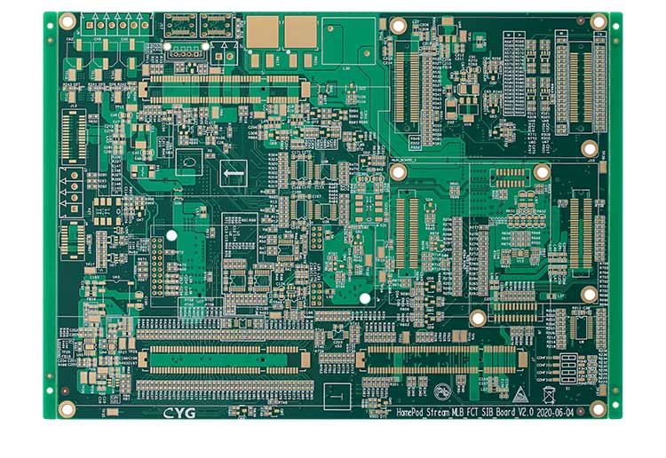
The blistering on the circuit board surface is actually the problem of poor bonding force of the board surface, which refers to the quality problem of the board surface. It contains two aspects:
1. The cleanliness of the board surface;
2. The problem of surface micro-roughness (or surface energy);
The blistering problems on all circuit boards can be summarized as the above reasons.
If the bonding force between the coatings is poor or too low, it is difficult to resist the coating stress, mechanical stress, and thermal stress generated during the production and processing, which will eventually cause different degrees of separation between the coatings.
Some factors that may cause poor board quality during production and processing are summarized as follows:
1.The problem of substrate processing:
Especially for some thinner substrates (generally below 0.8mm), because the rigidity of the substrate is poor, it is not suitable to use a brushing machine to brush the plate.
This may not be able to effectively remove the protective layer specially treated to prevent the oxidation of the copper foil on the board surface during the production and processing of the substrate. Although the layer is thin and the brush is easier to remove, it is difficult to remove it when it's used a chemical treatment, so in production, It is important to pay attention to control during processing, so as to avoid the problem of blistering on the board caused by poor bonding between the copper foil of the board substrate and the chemical copper.
2. The phenomenon of poor surface treatment caused by oil stains or other liquids contaminated with the dust during the machining (drilling, lamination, milling, etc.) of the board surface.
3.Poor plating through-hole of the printed board.
It will lead to the hole to be deformed when there is excessive pressure on the plate before electroless copper deposition, and therefore, it will cause blister in the hole in the process of electroless copper deposition, plating, hot air leveling as well as soldering, and so on. Even though there is leakage but the heavy brushing board will increase the roughness of the hole copper. Therefore, attention should be paid to strengthening the control of the brushing process. The brushing process parameters can be adjusted to the best through the wear scar test and the water film test.
4.Washing problem
The electroplating process for copper deposits has to go through a lot of chemical treatments, which are not easily cleaned by water. It will not only cause cross-contamination but also cause poor partial treatment of the board surface or poor treatment effect, uneven defects, causing some bonding problems.
Therefore, attention should be paid to strengthening the control of washing, mainly including the control of washing water flow, water quality, washing time, and plate dripping time; especially in winter, the temperature is lower, the washing effect will be greatly reduced.
5. Micro-etching in the pre-treatment of copper immersion and pattern plating:
Excessive micro-etching will cause leakage of the substrate in the orifice and cause blistering around the orifice. On the other hand, insufficient micro-etching will also cause insufficient bonding force and blistering; therefore, it is necessary to strengthen the control of micro-etching. Generally, the depth of micro-etching of the copper deposit is 1.5---2 microns, and the micro-etching before pattern plating is 0.3---1 micron. If possible, it is better to control the micro-etching thickness or the corrosion rate through chemical analysis and a simple test weighing method. The surface of the etched board is bright in color, uniform pink, with no reflection; if the color is not uniform, or there is a reflection, it means that there is a hidden quality problem in the pre-processing. Pay attention to strengthening the inspection; in addition, the copper content of the micro-etching bath, bath temperature, and load, Micro-etching agent content, etc. are items that also need to be paid attention to.
 PCB Assembly
 Layer Buildup
 Online Tools
 PCB Design-Aid & Layout
 Mechanics
 SMD-Stencils
 Quality
 Drills & Throughplating
 Factory & Certificate
 PCB Assembly Factory Show
Certificate


