
 NextPCB Capabilities
Printed Circuit Boards
NextPCB Capabilities
Printed Circuit Boards
 PCB Assembly
 Layer Buildup
 SMD-Stencils
 PCB Design-Aid & Layout
 Mechanics
 Quality
 Drills & Throughplating
 Factory & Certificate
 PCB Assembly Factory Show
Certificate
PCB Assembly Factory Show
Certificate
Support Team
Feedback:
support@nextpcb.com


There are four fundamental approaches to increasing the conductor capacity or connectivity of PWB density:
We will cover the impact of each strategy on designing yields and as a result PCB costs. The last approach is the easiest but most expensive if the ways tolerable for addressing the previous two conditions have proven fruitless to reach the desired board density.

Large pad widths around plated through-holes (PTHs) are the main impediments impeding an increase in conductor channel size. Since at the current state of technology, PWBs still require pads wider than the conductors at their site.
You should take into account the pads in order to properly analyze link density Id. Because these pads stop the affinity that PWB boards can achieve. For example, in one design, you can enhance the interconnection density by 50% more when you reduce the pad widths from 55 to 25 mils (by 55%).
Further, you can lessen the device conductor pitch (Cp) from 18 to 7 mils (by 61%). Now, it is obvious to you that a more effective technique to increase the wire capacity of a pad is to reduce or remove it entirely.
PWBs have copper pads around the drilled holes to accommodate any potential layer-to-layer or pattern-to-hole misregistrations. And it prevents any hole leave outside the copper area of the pads. There the two main causes of this misregistration. These are instability and movement of the base laminate during processing via the PWB or multilayer board (MLB) production processes.

According to base material features, this movement should be kept to a maximum of 300 ppm. But in practice, base material movement is more like 500 ppm. And this result in layer movement of 10 mils over a 20-in distance. This temperature is too broad for many applications. Because it helps at least a 10-mil-wide annular ring to around drilled holes, highly blurry device manager.
As we explained earlier, excessive material movement takes place if the laminating temperature is higher. That's why the laminate resin's glass transition temperature (Tg ) is another factor in MLB material instability. On the other hand, while the resin is still in its linear easy phase. There is a little dimensional fluctuation of the base material if the laminating temperature stays below the Tg of the resin.
Now, let's explain why high-Tg resins are required in the PWB sector. For example, the base material movement reduces to 200 from 500 ppm. And you can reduce the request for the annular ring width up to 4 from 10 mils. It is clear according to the data gathered from the performance of new and more stable one-way laminates.
Table. 2 shows the connectivity improvements made achievable by using a more stable laminate material. And it allows for a reduction in the starting diameters of the pads. As you can (see in the first column) separated at 1.5 mm (0.100 in) while maintaining the conductor pitches constant. Eliminating the pads and keeping the z-axis interlink inside the board of the device manager. It is important to produce the invisible vias to allow for the most productive use of the signal plane area.
So, this data is collected from the basis for this information. And which the engineers collect from the performance of newer and more authentic one way laminates. While all the engineers can use these traditional preparing techniques to create MLBs.
Table. 1 Effect of Pad Diameters on Interconnectivity Density:
| Pad dia, in | Cond Pitch, in | Id @ 500 ppm, in/in2 | Id @ 200 ppm, in/in2 | Id @ Invisible via, in/in2 |
|---|---|---|---|---|
| 0.055 | 0.010 | 20 | 37 | 55 |
| 0.036 | 0.018 | 30 | 48 | 55 |
| 0.025 | 0.009 | 40 | 96 | 100 |
| 0.025 | 0.007 | 60 | 130 | 143 |
And all manufacturers design all MLBs with these new and more size stable, side laminates and smaller pad sizes. Plus the creation of MLBs with invisible vias importance is the use of an important process. That is similar to the SLC process described earlier.
Although PWB manufacturers are generally at ease producing boards with 4- or 5-mil-wide conductors. So, they still need substantial pads surrounding plated holes to prevent hole breakout.
Table. 2 Effect of Increased Connectivity on Reduction of Layers:
| Pad dia, in | Cond Pitch, in | I |
I |
I |
|---|---|---|---|---|
| 0.055 | 0.010 | 10 | 6 | 4 |
| 0.036 | 0.018 | 7 | 4 | 4 |
| 0.025 | 0.009 | 5 | 2 | 2 |
| 0.025 | 0.007 | 4 | 2 | 2 |
You can check the most significant outcome of greater connection per layer in Table 2. According to this table, fewer signal layers are required to provide the same wiring density (Wd). And Table 1 is created by using linking information from Table. 2 applies to a 50-in2 MLB with 10,000 in total wiring length. Also, you should take note that the layer count in Table 2 has boosted to the next higher layer value. And it makes the computed 1.4 layers appear as 2 layers instead of the original value of 1.
When reducing the widths of device supervisor and spaces then increasing the number of accessible wire channels on each signal plane is possible. As previously mentioned, it is an apparent way to boost the connectivity of PWBs. The IC and PWB industries have been using this approach for a long time.
However, conductor widths or gaps cannot be reduced surely. The current-carrying capacity of thin, small managers limits the reduction in conductor width. Especially when these conductors are long, as they frequently are on PWB density. This conductor reduction has processing constraints. Because, if the reduction pushes the process capabilities above their regular limitations, manufacturing yields may suffer.

Additionally, there is a limit to how much the distances between the conductors can be reduced. Engineers determine this limit primarily by electrical considerations. For instance, one observes electrical limits by preventing excessive crosstalk, reducing noise, and providing suitable signal propagation conditions and characteristic impedance.
Nevertheless, if accomplished within the outlined boundaries. Then such conductor reductions can be a successful route for raising PWB density and lowering PWB manufacturing costs. The number of signal layers achieve the same connectivity when conductor widths are decreased from 6 to 3 mils.
It is present in Table 3, which is created by using cost data from the BPA's Columbus program. While we also maintain the same yields, interconnection density, and board area. This decrease in the number of layers has the potential to lower PWB board production costs dramatically.
TABLE.3 Effect of Conductor Widths on Number of Layers and Board Cost for a 6-in × 8-in MLB, with Id = 450 in/in2, 65 to 68 Percent Yields.
| Line-Space | Total No. of Layers | No. of Signal Layers | Board Cost, % |
|---|---|---|---|
| 3-3 | 8 | 4 | 55 |
| 4-4 | 10 | 6 | 64 |
| 5-6 | 12 | 7 | 77 |
| 5-7 | 14 | 8 | 87 |
| 6-6 | 16 | 8 | 90 |
| 7-8 | 20 | 10 | 100 |
It goes without saying that any effective increase in the conductor density Id in PWBs would only be possible. If the manufacturing methods allowed for production with acceptable yields. As it's shown in fig 1. When the PWB widths decrease below 5 mils, the yields of thin conductors also fall quickly.
FIGURE.1 Board yields versus conductor width:
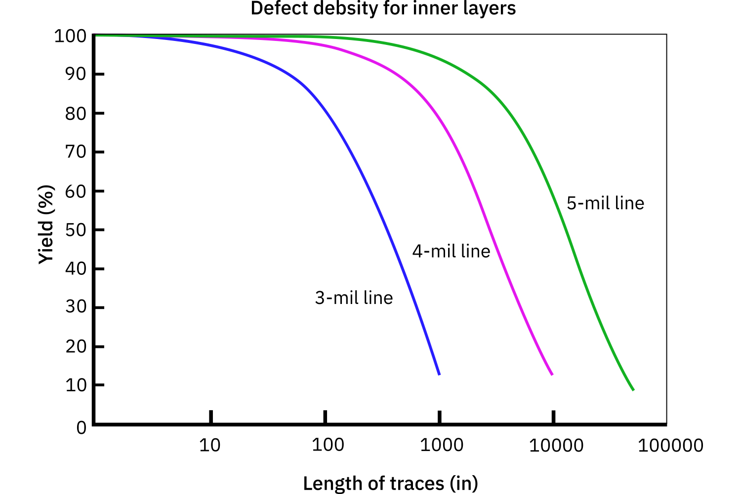
Because process yields have a significant impact on the price of interconnection substrates. So, understanding production yields is crucial for determining the most cost-effective manufacturing technique.
An effective empirical equation for determining the cost of production is:
$$Cost \: C=\frac{material+process\: cost}{yield \: Y}$$
Engineers can divide the total processing yield into two parts: one that depends on the conductor density, or Yid. And the second is a function of the combined yields of the other manufacturing processes. This will allow them to determine how the interconnection density Id affects the final yield of substrates:
Ytotal = YId*Yproc
A well-managed manufacturing process allows the yield function to be based only on changes in conductor widths. Because process-dependent yields (such as plating) are relatively stable for a particular technology.
FIGURE 2 Yield loss from shorts:
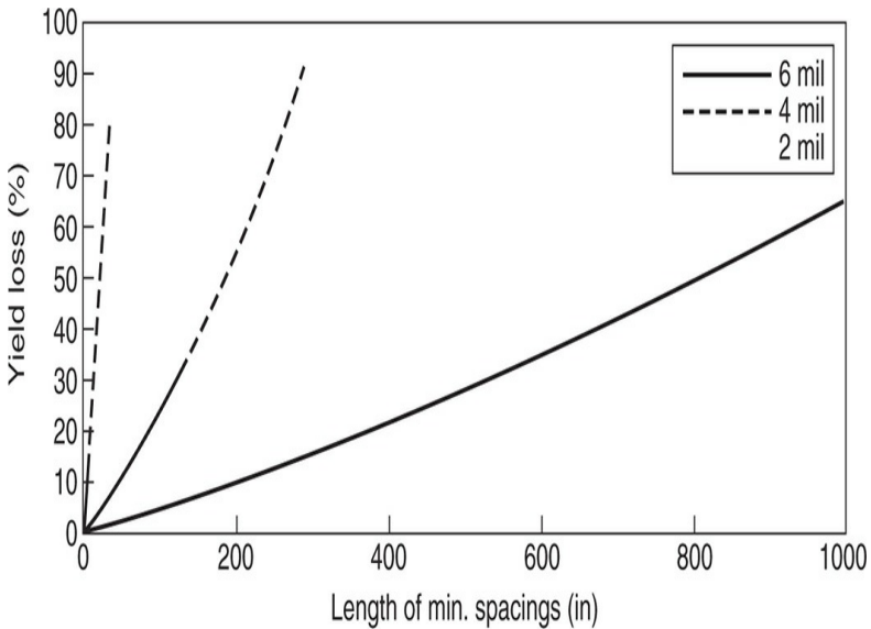
As you can see from Fig. 2. All conductor opens and shorts between them are the defects that have an impact on the density-dependent yield function Yid. It would be acceptable to assume that these flaws have a Poisson distribution. With an average defect frequency of v over the complete length TL of the substrate's conductors. The yield is the likelihood that the whole conductor length TL has no faults (n = 0).
Y = (at n=0) = e(−v*TL)(Poisson distribution)
As can be seen from Figs. 1 and 2, the defect frequency v depends on the conductor pitch Cp. As well as the widths of the lines and spaces. With a drop in Cp, will rise, but for very high Cp, ought to be zero since Yid will be 100%.
For instance, the interconnection density Id for a design with invisible pads. Where Cp = 2w, can be written as Id = TL/A. Id is proportional to Cp, so Id * Cp = 1, and TL = A/Cp. Consequently, this equation can be stated empirically as:
$$v=-ln \frac{Y_0}{TL_0}*( \frac{C_{p0}}{C_p})^b$$
where b is a factor that depends on the method or technique used to create the conductors. This component b must be empirically calculated for each situation. Because it varies greatly between facilities and among different pattern-generation techniques.
The simplest and clearest option is to simply add a layer when there isn't enough space on existing layers to place all interconnecting paths. Because this strategy has been widely used in the past.
But when the cost-effectiveness of the substrates is crucial, a very careful design study must be undertaken to reduce layer counts in MLBs. Because every extra layer in the board incurs a large cost rise. You can see from Table 3 that there is practically a linear relationship between board costs and layer count. For 6-in 8-in MLBs produced in large quantities with yields and conductor density held constant.
Figure 3 further explains that due to the requirement to interleave ground or DC power planes between signal planes. Any increase in the number of signal layers in boards operating at frequencies requiring transmission line features. That will result in double the total number of layers.
Fig. 3 of Cost relationships between the number of layers and conductor widths:
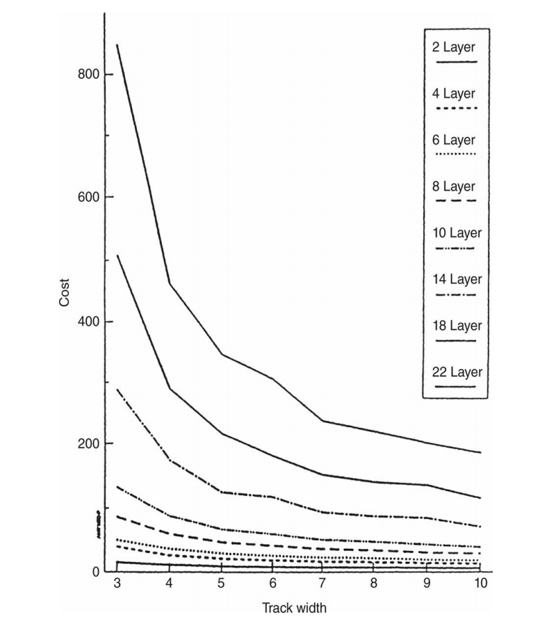
Increasing the number of layers in any of the line width categories results in a clear decline in manufacturing yields. This is a fairly common occurrence in the manufacture of circuit boards since MLB with more layers and a greater MLB complexity typically have more issues.
To sum up the discussion, everything is explained in detail about the PWB density and methods to increase it. We discussed it with different tables, charts, and equations. So, if you have any questions let us know in the below comment section. We will be pleased to answer you.
Still, need help? Contact Us: support@nextpcb.com
Need a PCB or PCBA quote? Quote now


 Surface

