
 NextPCB Capabilities
Printed Circuit Boards
NextPCB Capabilities
Printed Circuit Boards
 PCB Assembly
 Layer Buildup
 SMD-Stencils
 PCB Design-Aid & Layout
 Mechanics
 Quality
 Drills & Throughplating
 Factory & Certificate
 PCB Assembly Factory Show
Certificate
PCB Assembly Factory Show
Certificate
Support Team
Feedback:
support@nextpcb.com


In PCB design, some holes seem insignificant, but without these "tool holes", the board will not achieve the expected function or even be manufactured correctly.
Individually, the tool holes on the circuit board look very common because they are regular through holes drilled on the circuit board. Only by studying their functions carefully can we really understand their importance.
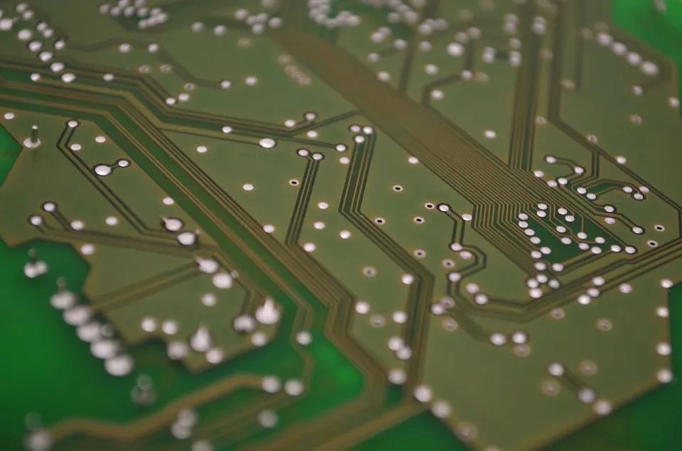
Some of these through-holes are used to connect the hardware to the circuit board, while the other part is used to help the manufacturing and assembly of the circuit board.
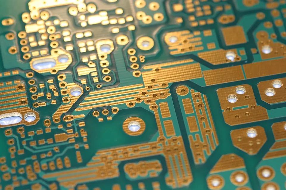
In the design and manufacture of PCB, many holes of different sizes are usually drilled on the board, which will be suitable for different functions.
Most holes are used to interconnect electrical signals between layers, and some holes are used to weld components and to install different hardware.
Tool holes (also known as "mounting holes") for connecting hardware can be associated with the package pattern of the component or marked separately.
In addition to soldering leads or pins to the circuit board, some components also have mounting hardware for increased physical support.
The connector is usually bolted to the board to protect its welded part from the pressure of cable plugging. Other components that are heavier or used as interfaces may also be tightened, including switches, fans, batteries and speakers.
These holes may also need to connect the mounting hardware to electrical ground or conduct heat through the board to disperse on the internal plane layer.
Finally, in order to install the PCB into its system, isolation holes are usually used to connect the hardware or bracket to be installed to the circuit board.
PCB tool holes can be placed on the board to facilitate cooperation with different manufacturing stages.
These holes guide the circuit board through its assembly processes, such as reflow soldering, wave soldering and automatic optical inspection (AOI). If the PCB requires additional testing, tool holes will also be used during the testing process.
If a tool hole is required on the plate during any manufacturing process, the manufacturer will require it to be added to the design.
Typically, the manufacturer will use existing holes in the plate or add them to the manufacturing file. The holes for mounting hardware are created and must be machined with the correct design parameters to perform the desired function:
Location: the number and location of machined holes depend on the requirements of the circuit board and components. The component datasheet usually specifies the location of these holes, which should be included in their PCB footprint by the designer.
Preferred size: this still depends on the requirements of the component. Typically, these parts will use 4-40 or 6-32 screws and must be drilled to match the mounting hardware. If the system mounting hole is not included in the design, the PCB manufacturer will generally recommend adding some holes with a general size of 0.100 or 0.125 inches to facilitate subsequent installation selection.
Plating: this depends on the hardware that needs to be installed. For hardware that needs to be electrically connected to the circuit board, the holes must be plated and connected to the appropriate network, otherwise, non plated holes should be used.
Plane connection: electroplated holes connected to the power supply or grounding plane shall not be connected to any other plane to prevent a short circuit between the power supply and grounding grid. Improperly designed mounting holes may eventually interfere with design rule checks.
Spacing: holes to accommodate mounting hardware usually need to have a large sheltered area around them. The mounting hardware needs enough space to firmly contact the circuit board without damaging the component lead or metal wiring and plane. Additional clearance around the electroplated hole is also crucial. The electroplated hole needs to be drilled larger so that the added electroplated material can finish the hole according to the required size.
Although tool holes and mounting holes do not seem to have much impact on PCB layout. But in fact, when designing and installing holes, we need to pay as much attention to details as PCB design. There are many elements in design that are also important for manufacturing.
In addition to the different PCB tool holes required for installing hardware and production aids, attention should also be paid to the design problems that may affect PCB manufacturing.
These include solder paste pads for surface-mounted component pins, solder resist films for protecting circuit boards, screen printed marks for component reference marks, and enterprise identification.
In addition, designers should also pay attention to the problem of reference pads. They are small pads used for PCB alignment during automatic assembly.
Reference pads are usually placed at the corners and center of large SMT devices with a high pin count. It may be challenging for designers to meet all the requirements for PCB manufacturing and assembly. But this is what an excellent PCB design engineer should do.
Still, need help? Contact Us: support@nextpcb.com
Need a PCB or PCBA quote? Quote now


 Surface


feet
There are many kinds of PCB hole, Via, through hole, blind hole, buried hole, partial depth hole, countersink hole, back drilling and press-fit hole, it's dizzy.