
 NextPCB Capabilities
Printed Circuit Boards
NextPCB Capabilities
Printed Circuit Boards
 PCB Assembly
 Layer Buildup
 SMD-Stencils
 PCB Design-Aid & Layout
 Mechanics
 Quality
 Drills & Throughplating
 Factory & Certificate
 PCB Assembly Factory Show
Certificate
PCB Assembly Factory Show
Certificate
Support Team
Feedback:
support@nextpcb.com


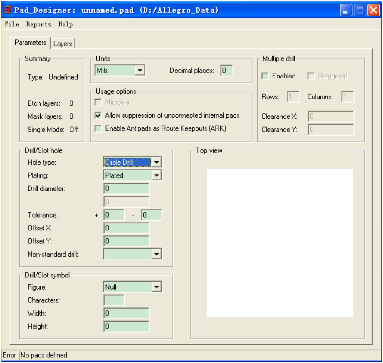
Select the unit in the Units drop-down box. Commonly used are Mils (millimeters) and Millimeter (millimeters). Choose according to the actual situation.
Select the type of drilling in the Hole type drop-down box. There are three options:
Select the metallization type of the hole in the Plating drop-down box. There are two commonly used ones:
Generally, the pin pads of through-hole components should be metalized, while the component mounting holes or positioning holes should be non-metalized.
Enter the drill diameter in the Drill diameter edit box. If you choose an ellipse or a rectangular hole, the two parameters Slot size X and Slot size Y correspond to the X and Y-axis radius of the ellipse and the length and width of the rectangle respectively. In general, it is enough to set the above parameters, and other parameters can be set by default. After setting, click the Layers tab to enter the interface as shown in Figure 1.2.
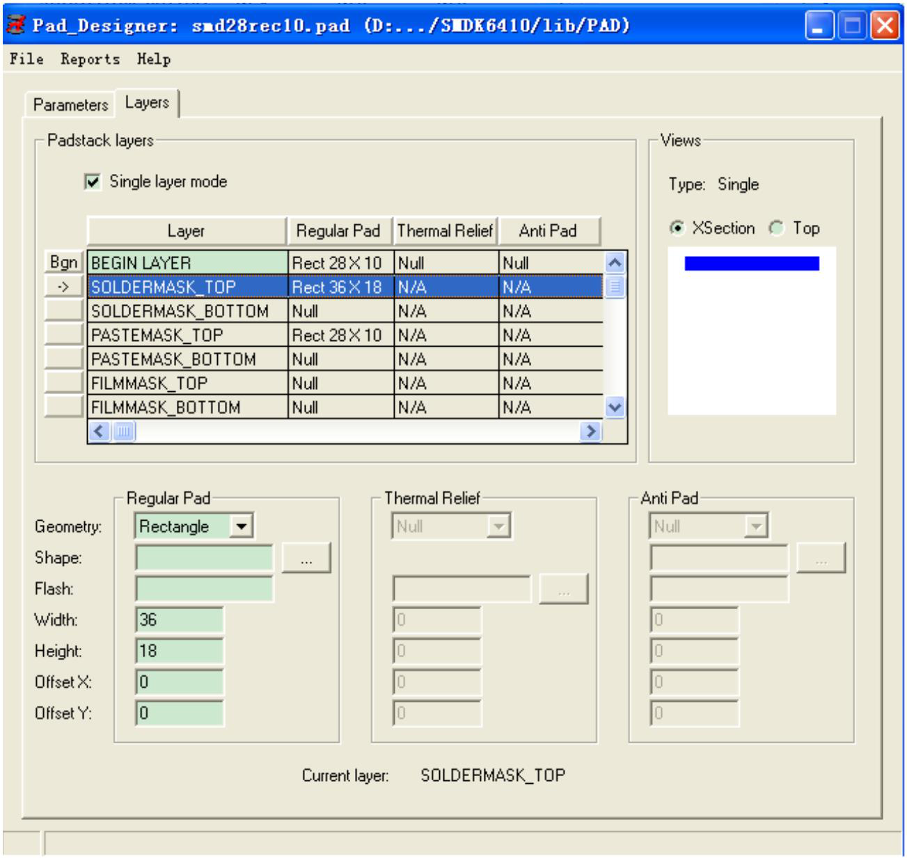
If you are making the pads of surface mount components, tick the Singel layer mode check box. Parameters to be filled in:
As shown in Figure 1.3.
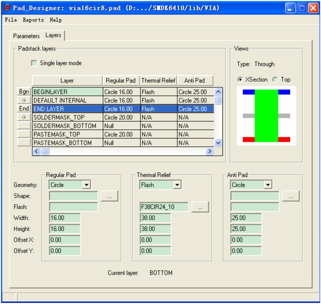
If it is a through-hole pad, the parameters that need to be filled are:
As shown in Figure 1.4.
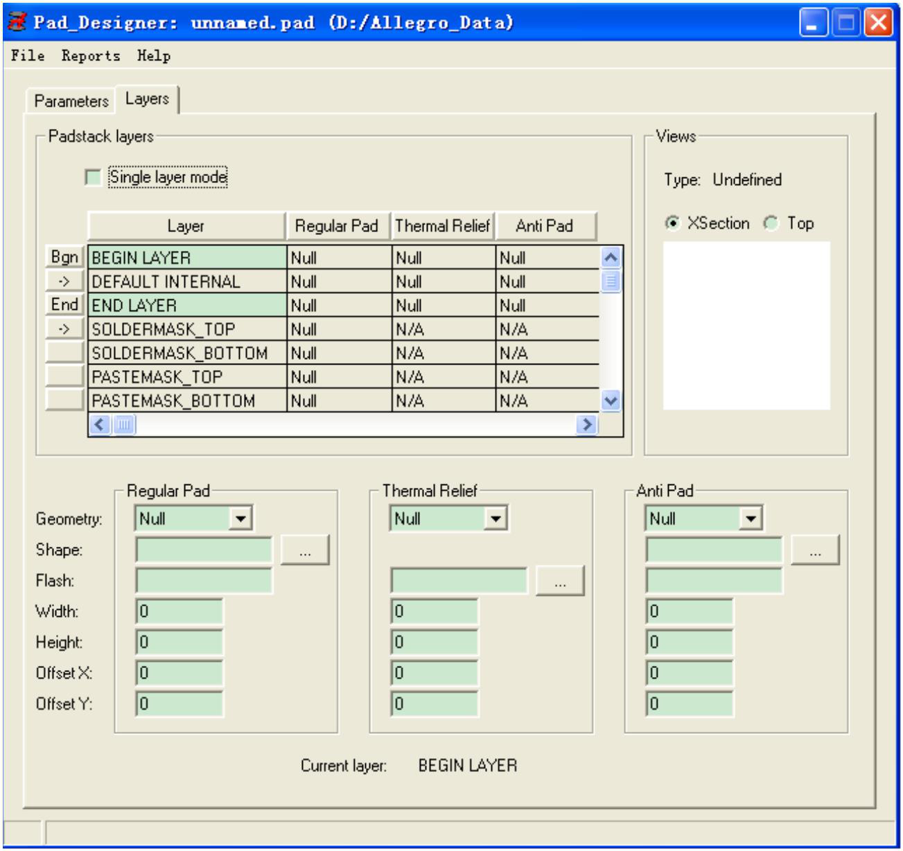
The Thermal Relief in the three levels of BEGINLAYER, DEFAULTINTERNAL, and ENDLAYER can choose the default connection methods provided by the system, namely Circle, Square, Oblong, Rectangle, and Octagon. In the PCB, these connection methods are simple '+' shapes. Or'X' shape. You can also choose your own hot air pad connection method, that is, choose Flash. This requires a Flash file to be prepared in advance (see Section 2). See the following introduction for the setting of these parameters.
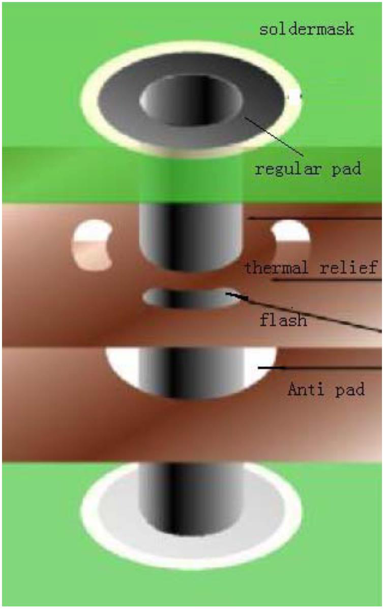
The following introduces some knowledge in a pad.
A physical pad contains three pads, namely:
Regular Pad: Regular pad, the pad seen in the positive film is also the basic pad of the through-hole pad.
Thermal Relief: Hot air pad, also called a flower pad, is effective in the negative film. It is used to connect the pad and copper in the negative film.
Anti Pad: An isolation pad, also effective in the negative film, is used to isolate the pad and copper in the negative film.
SOLDEMASK: Solder mask, where the copper skin is exposed and needs to be soldered.
PASTEMASK: The size of the steel mesh window.
Selection of land name level size of surface mount component package:
Same as BEGINLAYER layer setting.
The parameters of this layer are set as follows:
DRILL_SIZE >= actual pin size + 10MIL
Regular Pad >= DRILL_SIZE + 16MIL (0.4mm) (DRILL_SIZE<50)
Regular Pad >= DRILL_SIZE + 30MIL (0.76mm) (DRILL_SIZE>=50)
Regular Pad >= DRILL_SIZE + 40MIL (1mm) (when the drilling is rectangular or oval)
Thermal Pad = TRaXbXc-d where TRaXbXc-d is the name of Flash (described later)
Anti Pad = DRILL_SIZE + 30MIL (0.76mm)
SOLDERMASK = Regular_Pad + 6MIL (0.15mm)
Flash Name: TRaXbXc-d
in:
a. Inner Diameter: Drill Size + 16MIL
b. Outer Diameter: Drill Size + 30MIL
c. Wed Open: 12 (when DRILL_SIZE = 10MIL or less)
15 (when DRILL_SIZE = 11~40MIL)
20 (when DRILL_SIZE = 41~70MIL)
30 (when DRILL_SIZE = 71~170 MIL)
40 (when DRILL_SIZE = 171 MIL or more)
Ensure that the width of the joint is not less than 10mil.
d.Angle:45
When making the pad, it must be noted that the size of the Anti Pad must be larger than the Regular Pad, otherwise, the copper-clad layer will cause a short circuit. Because allegro's file management is a bit mixed, each pad will be saved in a file, so when naming the pads, try to show the shape and size of the pads, so that it can be easily managed and reused in the future.
Open Program->Cadence SPB 16.2->PCB Editor, select File->New, as shown in Figure 1.6.

The New Drawing dialog box pops up, as shown in Figure 1.7.
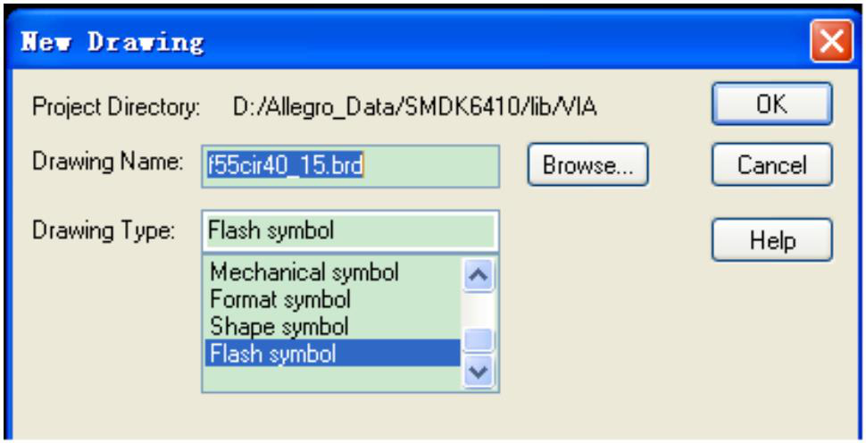
Enter the file name f55cir40_15 in the Drawing Name edit box, the suffix name is automatically generated. Select Flash symbol in the DrawingType list box, and click OK.
Click Setup->Design Paramenters to open the design parameter setting dialog box, and click the Design tab, as shown in Figure 1.8.
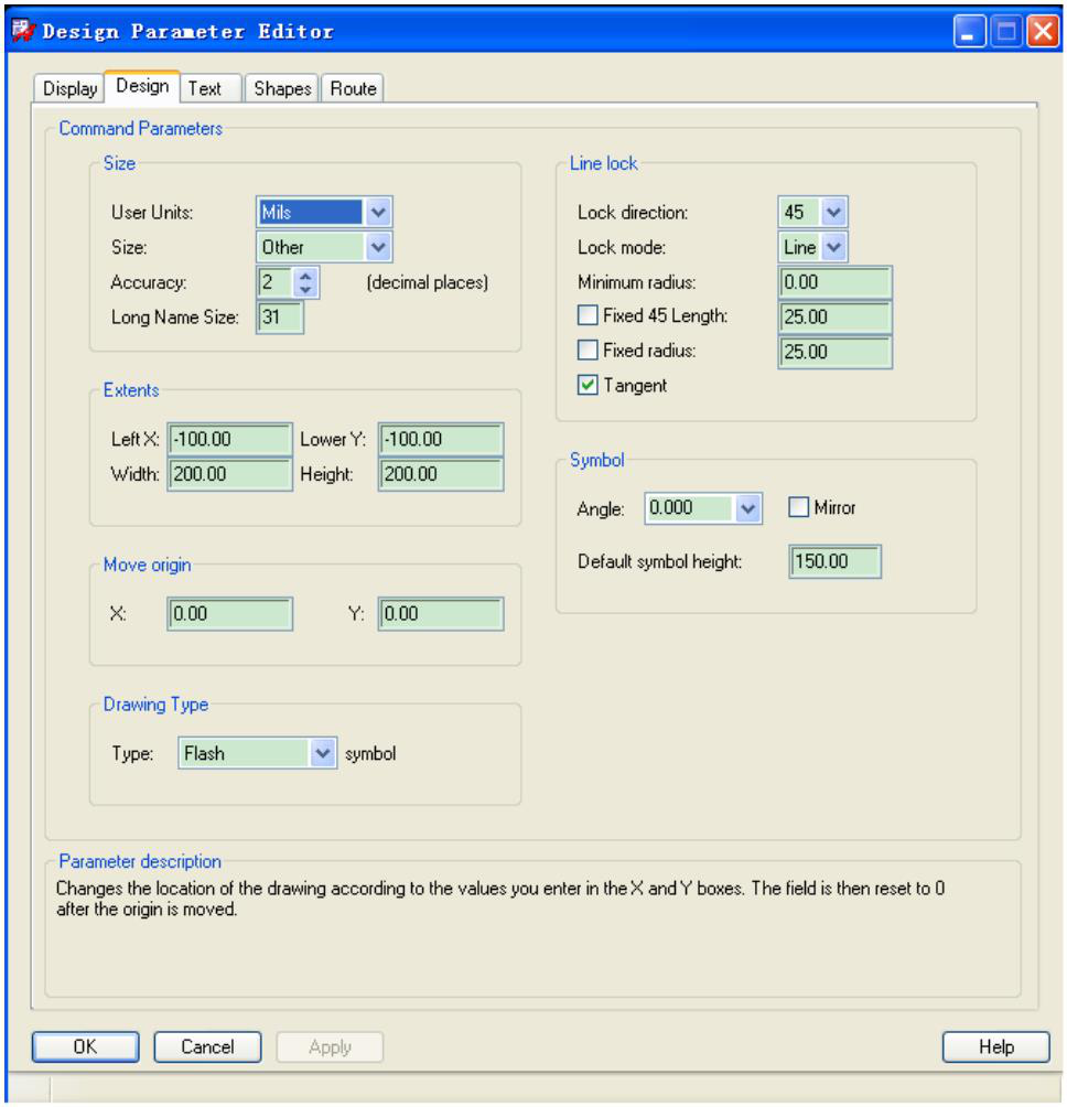
Select the unit Mils in User Units. In Accuracy, set the number of decimal places. The default is two digits. Enter 200 for Width and 200 for Height to set the size of the drawing area. You can adjust the size appropriately according to the pad you made, then enter -100 for Left X and -100 for Lower Y to set the coordinates of the lower-left corner of the drawing area, So that the origin coordinate (0, 0) is at the center of the drawing area, otherwise there will be errors. Use the default values for other parameters, and then click OK to exit.
Click Add->Flash menu to pop up the hot air pad size setting dialog box, as shown in Figure 1.9.
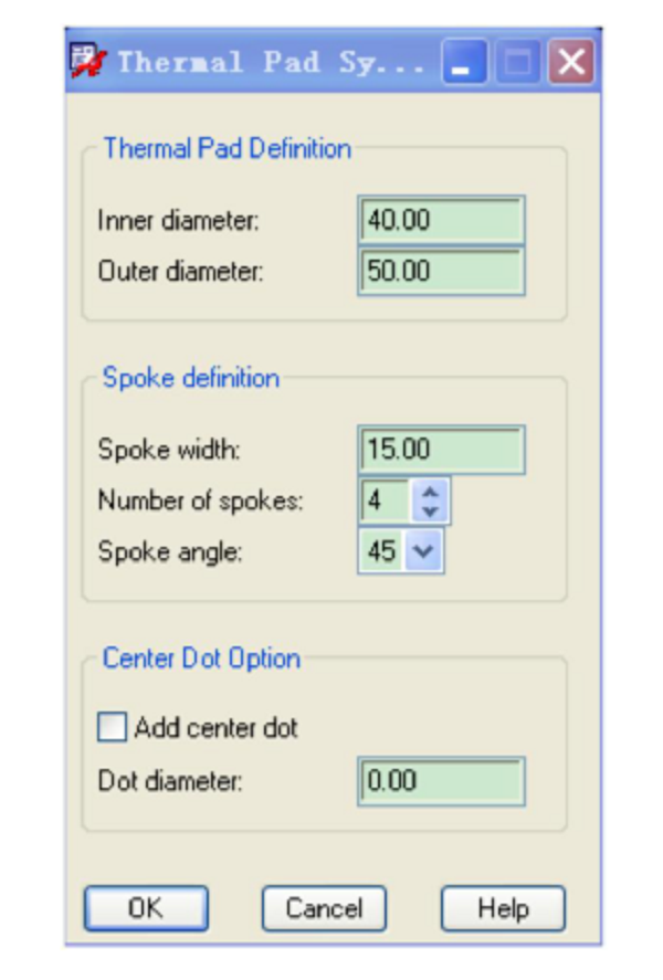
Enter the inner diameter 40 in the Inner diameter edit box, enter the outer diameter 50 in the Outer diameter edit box, and enter the connection width 15 in the Spoke width edit box. It is best not to be less than the minimum line width of the board. Select the number of openings in the Number of spokes, the default is 4, and the Spoke angel input opening angle is the default 45 degrees. Other defaults, after clicking OK, a flower pad shape will be automatically generated, as shown in Figure 1.10.
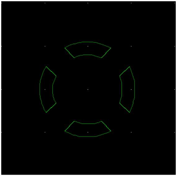
At this point, a circular hot air pad is completed. If you want to generate other shapes of pads, such as oval, square, etc., you cannot use Add->Flash to generate it. You need to use the draw rectangle and circle tools under the Shape menu Come draw. First, draw a sketch by yourself, and calculate the coordinates of each point, and then use commands such as drawing rectangles and circles and enter the coordinates in the command status bar to draw. It should be noted that since the hot air pad is used in the negative film, the place you can see the shape is drawn (the area enclosed by the green line in Figure 1.10) is actually corroded after the PCB is made, and the black (bottom) Color) is where there is really copper.
Still, need help? Contact Us: support@nextpcb.com
Need a PCB or PCBA quote? Quote now


 Surface


vsee
Nice page about PCB pad making. For through-hole components, the pad is usually circular, and there will be a plated hole through it for inserting and soldering component leads. For surface mount technology (SMT) parts, the size and shape of the pads will vary depending on the components to be soldered