Support Team
Feedback:
support@nextpcb.com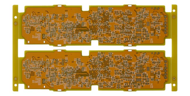
Material: SYTECH
Layer Count: 4 layers
PCB Thickness: 1.6mm
Min. Trace / Space Outer: 0.1mm/0.1mm
Min. Drilled Hole: 0.2mm
Via Process: Tenting Vias
Surface Finish: ENIG+OSP
1. DK needs to be tiny as well as steady sufficient, typically the smaller sized the much better, high DK might cause signify transmission hold-up.
2. DF ought to be little, which mostly influences the top quality of signal transmission, the smaller sized DF might make smaller sized signal waste as necessary.
3. The thermal expansivity ought to coincide with copper aluminum foil as long as feasible, due to the fact that the distinction will certainly result in copper aluminum foil divided in the modifications of cool and also warm.
4. Water absorptivity has to be reduced, high water absorptivity will certainly influence DK as well as DF when in the damp atmosphere.
5. Heat-resisting property, chemistry resisting, impact endurance, peel-off resisting must be good. Materials used for HF circuit board.
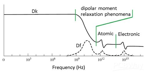
1. Adjusted permittivity.
2. Reduced depletion for reliable signal transmission.
3. Uniform building and construction with reduced resistances in insulation density as well as dielectric continuous.
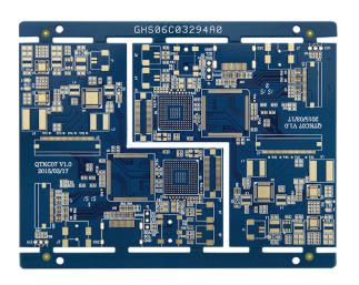
Material: Fr-4
Layer Count: 6 layers
PCB Thickness: 1.0mm
Min. Trace / Space Outer: 0.075mm
Min. Drilled Hole: 0.1mm
Via Process: Tenting Vias
Surface Finish: ENIG
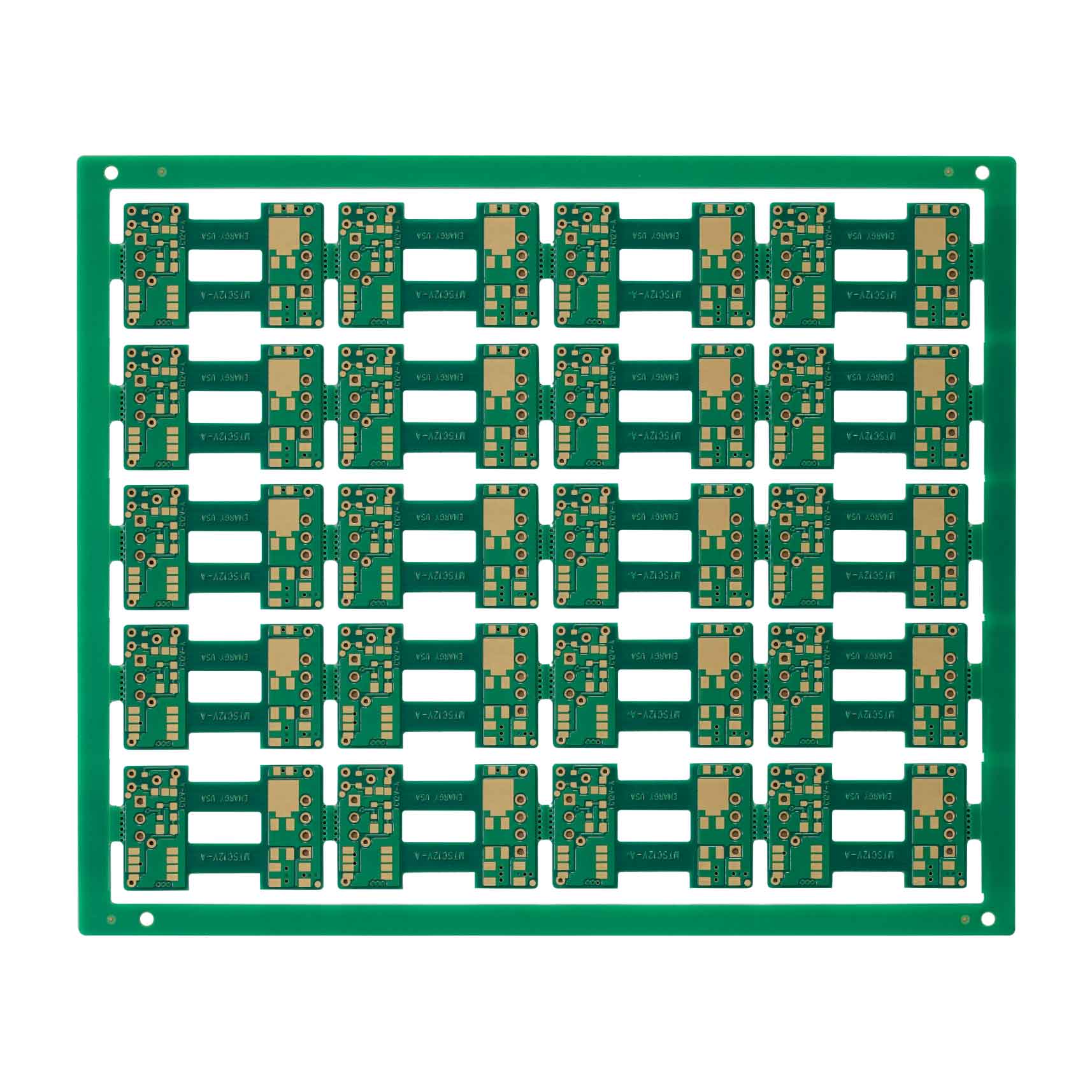
Material: Fr-4
Layer Count: 6 layers
PCB Thickness: 1.6mm
Min. Trace / Space Outer: 3/3mil
Min. Drilled Hole: 0.25mm
Via Process: Tenting Vias
Surface Finish: ENIG
PCB is the abbreviation of the...


