
 NextPCB Capabilities
Printed Circuit Boards
NextPCB Capabilities
Printed Circuit Boards
 PCB Assembly
 Layer Buildup
 SMD-Stencils
 PCB Design-Aid & Layout
 Mechanics
 Quality
 Drills & Throughplating
 Factory & Certificate
 PCB Assembly Factory Show
Certificate
PCB Assembly Factory Show
Certificate
Support Team
Feedback:
support@nextpcb.com


Etch refers to the trace and shape in Allegro software, and Shape refers to copper skin.
The Etch on the trace layer of the positive film refers to the drawn line and shape, etc. The part you see is the place where there is copper.
In the negative film layer, Allegro software uses the Antietch line as the separation line between the Shape and the Shape. After the negative film layer is covered with copper, there is no copper where there is the Antietch line, and there is no copper area without the Antietch line.
Q: What is the use of Antietch? Is it necessary to divide power and ground? Will it cause a short circuit if Antietch is not used during power split?
Answer: It is used for the division of the negative film. The negative film is divided into two or more parts, and it can be automatically laid copper. It is more convenient to divide the copper after the copper has been laid. You can use it for the shape of the divided copper. Create the shape of the Shape, you can also use Void, Edit Boundery and so on, and use it flexibly.
Q: In other words, if it is a positive film, you don't need Antietch, you only need Etch. Can you think of it this way? There is also whether the positive film or the negative film is for Gerber output, to determine it?
Analysis: In Xsection, you must first set Plane, Negative and then select Negative when you exit Gerber; adding Antietch is to facilitate Plane layer segmentation. Antietch is not required for the positive film layer.
Q: Can positive and negative films coexist in the same BRD file? For Antietch, it is convenient to divide the Plane layer, and how to understand it.
Analysis: The Plane layers are all set to negative film layers. Negative film layer segmentation is easy to do with Antietch, which can be split automatically, and the copper foil does not need to be painted by hand; general PCBs have positive and negative films, and the positive and negative films can exist in the same brd at the same time.
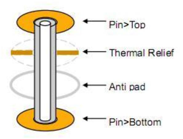
Q: PTH hole connection problem
Analysis: Connected to the positive film, ALLEGRO takes REGULAR PAD. It has nothing to do with others; it is connected to the negative film layer, which is Thermal Relief, and it has nothing to do with the other; it is isolated from the negative film layer, which is used as Anti Pad.
Q: Under what circumstances are positive and negative films used separately, what is the difference between them, and what does "negative film layer isolation" mean?
Analysis: The understanding of Thermal Relief is to prevent the pad from overheating and cause false soldering. The positive film is connected to the Regular Pad and has nothing to do with others.
Negative film layer isolation: For example, on the GND layer, if there is a PTH hole that is not connected to GND, then it needs to be isolated from GND. At this time, the size of the isolation is Anti Pad, which has nothing to do with others.
Thermal Relief: Mainly to control the heat spread of the Pad, it is too fast to rework. The negative film is basically the power ground, and the positive film is basically the wiring layer. This makes it easy to distinguish.
Q: Is it easy to make mistakes when the positive and negative films are in the same BRD file at the same time?
Analysis: On the Vendor side, positive Gerber can also be made into negative film, and negative film can also be made into positive film. It is understood that when PCB is made, Vendor will determine the positive and negative film of the film according to their needs.
Q: Is the power layer set to negative film better than positive film? Why should the power plane be set as a negative film?
Analysis: When the negative film isolates the PTH, the PTH hole does not have a regular pad on the negative film layer, which is very good for the signal. The feature film has Regular Pad. The smaller the distance between the pad and the power supply and ground is not good for the signal. There is no difference between positive and negative film for the manufacturer's production. Any PCB design software has a positive and negative film area.
Analysis: Antietch is used to draw the inner isolation line, which is a line with no electrical characteristics, while Etch is a line with electrical characteristics and is usually used.
Q: When Antietch does not cut to the edge of the board completely, there is still a little space left, so is there a way to check it out?
Analysis: In the Available Films in Artwork, assign the Antietch layer to the corresponding negative film layer. Draw a circle of Antietch along the edge of the negative film first, with a width of 0.5MM or more; when dividing the negative film, the Antietch joints are overlapped; and the negative film copper skin is laid.
Set Package KeePin and Route KeePin away from the Board Outline.
When setting the color in Allegro, one of the items is Antietch. What is this? Does Etch mean trace? Does it want to be used with Trace in PADS? It is a layer of negative film layer used to draw dividing lines. In the future, when running the negative film layer, these lines will separate the Shape, which is commonly known as the ink line. When the Gerber is produced, if the negative film is produced in the inner layer, only the ink line will be output. When the PCB board factory is exposing, only the ink line part will be exposed.
The positive film actually exists if it can be seen on the negative film; the negative film actually does not exist when it is seen on the negative film. The positive film and the negative film are opposite from the name. The following two pictures best illustrate the difference and are easy to understand.
The advantage of the positive film is that if the moving components or vias need to be re-plated with copper, there is a more comprehensive DRC verification.
The advantage of the negative film is that there is no need to re-lay the copper to move the components or vias, the copper is automatically updated, and there is no comprehensive DRC verification.
You can see the hot air pads in the picture above, which are divided into positive hot air pads and negative hot air pads.
Still, need help? Contact Us: support@nextpcb.com
Need a PCB or PCBA quote? Quote now


 Surface

