
 NextPCB Capabilities
Printed Circuit Boards
NextPCB Capabilities
Printed Circuit Boards
 PCB Assembly
 Layer Buildup
 SMD-Stencils
 PCB Design-Aid & Layout
 Mechanics
 Quality
 Drills & Throughplating
 Factory & Certificate
 PCB Assembly Factory Show
Certificate
PCB Assembly Factory Show
Certificate
Support Team
Feedback:
support@nextpcb.com


For PCBs with four or more layers, different suppliers offer distinct stack-up structures. At NextPCB, customers can choose among three standard four-layer stack-up options at no extra cost for production. However, deviations from these standard stack-ups will incur an additional cost of at least $80. NextPCB's DFM software facilitates 50-ohm impedance control for traces under any stack-up configuration.
Impedance matching is fundamental to ensuring signal integrity (SI) and power integrity (PI), directly affecting the speed, quality, and efficiency of signal transmission. Improper impedance values can lead to signal reflections and increased crosstalk, which in turn degrade circuit performance and, in severe cases, may even cause system failure. Therefore, precise impedance control is critical in high-speed digital circuits and high-frequency RF designs.
The reason why 50 ohm impedance has become the industry standard is the result of technical optimization and industrial development. Deviation from this value can cause signal reflections, distortion and data integrity issues, especially at high frequencies. The choice of 50 ohms is essentially a balance between technical ideals and engineering realities. From military requirements during World War II to today's 5G communications, this value has always represented the best balance between power handling, signal loss and cost.
Trace DC resistance is primarily governed by copper length, cross-sectional area (width x thickness), resistivity (ρ), and temperature. Substrate properties, trace spacing, and interlayer distance primarily impact impedance and AC performance. Frequency markedly increases effective resistance via skin effect.
> Recommend reading: PCB Antenna Layout & Keep-out Design: Best Practices for IoT Hardware
Let me walk you through a customer example using our DFM software. I'll show how you can achieve a 50-ohm trace on each layer without adding cost. This calculator is a particularly good fit for NextPCB manufacturing.
Customer Data:
·Stack-up: 2116
·Trace Width: 7.91 mil
·Distance to Copper: 15.75 mil
·Impedance Model: Coplanar Single-ended
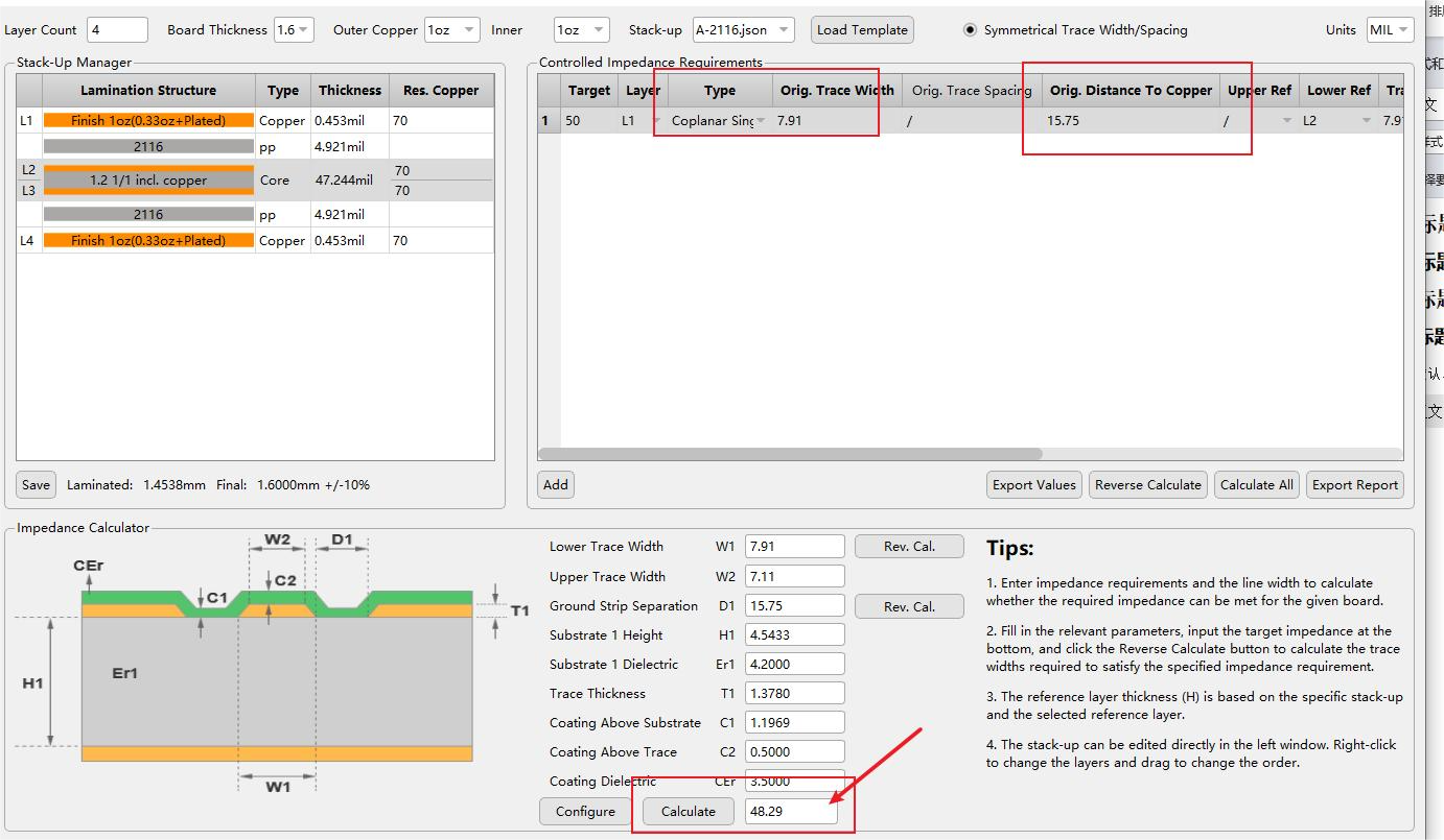
As shown, we input the customer’s data under stack-up 2116 and click "calculate," resulting in an impedance of 48.29 Ohms, which is slightly below the required 50 Ohms. Since the customer requires stack-up 2116 and the impedance model of Coplanar Single-ended to remain unchanged, we can only adjust the trace width of 7.91 mil and the distance to copper of 15.75 mil.
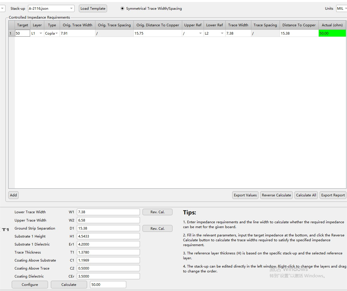
To achieve a higher impedance value, we need to incrementally reduce these two values. Through continuous testing, we find:
·Trace Width = 7.38 mil
·Ground Separation = 15.38 mil
In this case, the impedance reaches 50 Ohms.
Want to learn more? We have a dedicated article on PCB impedance. If your design has other impedance control requirements, feel free to reach out to our tech team anytime for support.
Still, need help? Contact Us: support@nextpcb.com
Need a PCB or PCBA quote? Quote now


 Surface

