NextPCB Capabilities
Printed Circuit Boards
NextPCB Capabilities
Printed Circuit Boards
 PCB Assembly
 Layer Buildup
 SMD-Stencils
 PCB Design-Aid & Layout
 Mechanics
 Quality
 Drills & Throughplating
 Factory & Certificate
 PCB Assembly Factory Show
Certificate
PCB Assembly Factory Show
Certificate
Support Team
Feedback:
support@nextpcb.com


Introduction
A sample and hold circuit is a fundamental component in analog electronics, used to capture and preserve voltage or current levels. It acts as a temporary storage device, 'sampling' the input signal and then 'holding' that value until it is ready to be processed or converted. This circuit is commonly used in applications such as analog-to-digital converters (ADCs), where it helps maintain the accuracy of the conversion process. The sample and hold circuit consists of two main parts: the sample switch and the hold capacitor. The sample switch connects the input signal to the hold capacitor, allowing it to charge up and store the voltage or current level. Once the sample switch is turned off, the hold capacitor maintains the stored value, preventing any changes caused by the input signal. This process makes sure that the analog signal is shown accurately when it's changed or sent, reducing mistakes and keeping the original information intact.
Sample and Hold circuits find extensive applications in various fields. In analog-to-digital converters, for instance, they are used to sample the continuous analog input signal before quantizing it into discrete digital values. In communication systems, Sample and Hold circuits help reconstruct analog signals from their digitized counterparts, contributing to high-quality signal processing. Additionally, these circuits are employed in radar systems, medical instrumentation, and audio processing, among other areas where precision in signal sampling is paramount. Let's explore the basics of a Sample and Hold Circuit—an important part of analog electronics. This article covers its circuit diagram, why it's important, how it works, the waveforms it deals with, how to connect it, its functional diagram, performance measures, where it's used, and wraps up with a conclusion.
Components Free Worldwide Shipping
In our sample and hold circuit diagram, we use a 2N4339 transistor, an op-amp (741), and a capacitor. The command input, a PWM signal, connects to the transistor's Gate. A diode is placed between the command input and the transistor, and it's set up in reverse because of how the transistor works.
The 2N4339 transistor turns on when the command input is negative, allowing it to conduct. We've set it up so that when the command input is high, the transistor acts like a closed switch, and the capacitor charges to capture a sample of the input signal. When the command input is low, the transistor acts like an open switch, creating high impedance. This stops the capacitor from losing its charge, holding the sampled signal for a specific period called the Holding Period. The time during which the circuit captures the input signal is known as the Sampling Period.
We're using the Op-amp 741 as a voltage follower because it has a high input impedance and low output impedance. This helps when the input signal has low current, as the voltage follower can provide enough current to the next stage in the circuit. Overall, this setup allows us to effectively sample and hold the input signal in our circuit.
The significance of a sample and hold circuit lies in its ability to overcome the limitations of analog signals. Analog signals are continuously varying, making it challenging to capture their precise values. However, by using a sample and hold circuit, the signal can be "frozen" or "sampled" at a specific moment, ensuring that the value is accurately measured. We use sample and hold circuits in ADCs. ADCs convert analog signals into digital form, which can be processed by digital systems. The sample and hold circuit is responsible for holding the analog input voltage constant during the conversion process, ensuring that the converted digital value accurately represents the original analog signal.
We can also use sample and hold circuits in data acquisition systems. These systems are used to measure and record various physical quantities, such as temperature, pressure, or voltage. The sample and hold circuit is used to capture the analog signals from sensors and hold them steady until they are converted into digital form for further analysis or storage. The sample and hold circuit are fundamental components in electronic systems that deal with analog signals. Their ability to freeze and hold the analog signal at a specific moment in time is crucial for accurate measurements and reliable data acquisition. Without sample and hold circuits, the conversion and processing of analog signals would be significantly compromised.
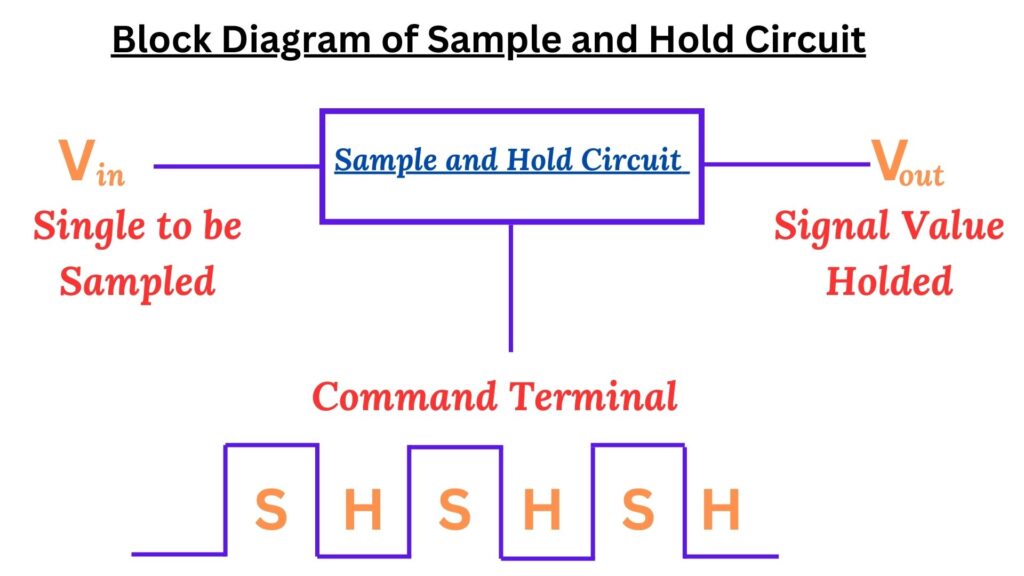
Understanding how a sample and hold circuit works is like figuring out the roles of its main parts. Imagine it as a team with three key players: an N-channel Enhancement MOSFET, a capacitor, and a high-precision operational amplifier. The MOSFET is like a switch, acting similar to a traffic light. It follows the orders of the input voltage through the drain and the control voltage through the gate. When it gets a positive control voltage pulse, it turns ON, becoming a closed switch. Conversely, when the control voltage is zero, it turns OFF, becoming an open switch.
When the MOSFET is in the closed-switch state, the analog signal flows to the capacitor through the drain. The capacitor quickly charges to its highest level. But when the MOSFET opens, the charging stops. Thanks to the operational amplifier with its high impedance, the capacitor holds onto the charge, preventing it from disappearing. This holding period is crucial as it retains the sampled value.
At the same time, the moments when the input voltage is sampled are called the sampling period. The operational amplifier doesn't just sit around; it's busy during the holding period, processing the output and making sure the circuit runs smoothly. So, the sample and hold circuit is like a well-coordinated team, capturing and holding onto the right moments in the input signal for further use.
In simple terms - Sample and Hold circuit efficiently captures and holds analog signals using the interplay between the MOSFET, capacitor, and operational amplifier. The MOSFET acts as a switch, the capacitor stores the charge, and the operational amplifier ensures the integrity of the held signal during the holding period, making it a crucial component in various electronic applications.
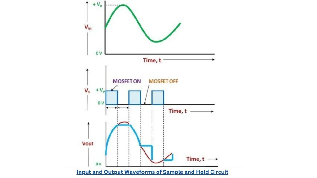
The input and output waveforms of a Sample and Hold (S&H) circuit are crucial aspects that illustrate its functioning. Let's explore the characteristics of these waveforms:
Input Waveform: The input waveform to a Sample and Hold circuit is typically an analog signal. This can be a continuous waveform representing varying voltage or current levels over time. The key feature of the input waveform is its continuous nature, reflecting the real-world analog signal that needs to be sampled and preserved.
Sampling Phase: During the sampling phase, which is controlled by the S&H circuit, specific snapshots or samples of the input waveform are captured at regular intervals. These samples represent the instantaneous values of the analog signal at those specific moments in time.
Output Waveform: The output waveform of the S&H circuit is characterized by discrete levels or steps. In the ideal scenario, during the holding phase, the S&H circuit maintains the sampled value constant until the next sampling cycle. This leads to a step-like output waveform, where each step corresponds to a sampled value.
Hold Period: The time during which the output waveform remains constant is known as the hold period. During this interval, the S&H circuit ensures that the sampled value is preserved without any changes. The output waveform retains these discrete levels until the next sampling phase begins.
Reconstruction in DACs: In applications where the output of the S&H circuit is further processed or converted, such as in digital-to-analog converters (DACs), the discrete levels of the output waveform may be reconstructed into a smoothed, continuous signal. The output of the DAC would then approximate the original analog input waveform.
The schematic layout provides valuable insights into how the input voltage and control voltage are intricately linked within the Sample and Hold circuit, offering a clearer picture of their application to the operational amplifier (OP-AMP). Choosing a versatile capacitor is vital, ensuring it has minimal leakage. Capacitors made of materials like Teflon and polyethylene prove suitable for achieving the intended purpose. The connection diagram prominently features the LF 398, a specialized integrated circuit designed for Sample and Hold applications. This IC plays a central role in the architecture of the circuit, facilitating its effective operation.
A noteworthy consideration in this setup is the frequency of both the analog input signal and the control signal. Ensuring the efficiency of the Sample and Hold circuit requires careful attention to these frequencies. Specifically, the frequency of the control voltage should surpass that of the input voltage. This strategic arrangement ensures that the analog signal undergoes sampling twice within a complete cycle, a crucial aspect for maintaining the circuit's effectiveness.
The functional diagram of a Sample and Hold (S&H) circuit gives a visual representation of its essential components and how they work together. Understanding this diagram provides insights into how the sample and hold circuit captures and maintains the input signal, ensuring accurate and controlled signal processing. It's crucial for the sample switch, hold capacitor, control logic, and timing elements to coordinate effectively for the circuit to operate reliably. Here's a brief overview of the functional diagram:
Key Performance Parameters of Sample and Hold Circuit:
Acquisition Time (TAC): Acquisition time, denoted as TAC, represents the duration it takes for the capacitor in the sample and hold circuit to accumulate the charge from the applied input voltage. Essentially, it is the time required for the circuit to capture and store the instantaneous value of the input signal. A shorter acquisition time is generally preferable as it ensures a more rapid and accurate response to changes in the input signal.
Aperture Time (TAP): Aperture time, or TAP, characterizes the time taken by the capacitor to transition from the sampling phase to the holding phase. Due to the inherent propagation delays in switches, the capacitor may continue to charge briefly even after the hold command is initiated. This residual charging time is termed aperture time. Minimizing aperture time is essential for enhancing the precision of the Sample and Hold circuit, ensuring a swift and accurate transition between sampling and holding phases.
Voltage Droop: Voltage droop refers to the reduction in voltage across the capacitor caused by the leakage of charge. While ideal capacitors would exhibit no leakage, practical considerations mean that some voltage drop occurs. Despite using high-quality materials, capacitors inherently experience a small amount of charge leakage, leading to a gradual decrease in voltage over time. Controlling voltage droop is crucial for maintaining the integrity of the sampled signal and sustaining circuit accuracy.
Hold Mode Settling Time: After the initiation of hold commands, the analog input voltage, utilized by the capacitor for charging during the sampling phase, requires a certain duration to settle completely. This settling time, known as hold mode settling time, is a critical performance parameter. Reducing hold mode settling time is desirable for achieving faster stabilization of the capacitor's stored charge and ensuring the circuit's readiness for subsequent operations.
The Sample and Hold circuit is a fundamental building block that allows us to capture and store an analog signal at a specific instant in time, and then hold that value until it is required for further processing. Here are some of the key applications of the Sample and Hold circuit.
As just discussed, sample and hold circuits are used in Radar Systems, Communication systems, Control system, Analog-to-Digital Conversion and Signal Reconstruction in Data Communication. That is why there are many important applications and use of sample and hold circuits.
In conclusion, the sample and hold circuit is a vital component in electronics, crucial for signal processing and data acquisition. Its ability to accurately sample and hold an input signal, showcased in applications like analog-to-digital converters, is pivotal. We explored its working principles, emphasizing precise retention of sampled voltage levels during the holding phase. Proper connections and a functional diagram are essential for effective operation, while key performance parameters guide circuit selection. From preventing signal degradation to ensuring consistency in various applications, the sample and hold circuit proves invaluable. Engineers can optimize electronic systems by understanding its circuitry, principles, and applications.
- How To Read Electrical Schematics
- 12 Commonly Used Components on PCBs for Beginners
- Free Worldwide Shipping on Over 600,000 Electronics Components with HQ Online
- Free PCB Assembly Offer is Now Live: Experience Reliable PCB Assembly from HQ NextPCB
- HQ NextPCB Introduces New PCB Gerber Viewer: HQDFM Online Lite Edition
Still, need help? Contact Us: support@nextpcb.com
Need a PCB or PCBA quote? Quote now


 Surface