

 PCB Assembly


Julia Wu - Senior Sales Engineer at NextPCB.com

 NextPCB Capabilities
Printed Circuit Boards
NextPCB Capabilities
Printed Circuit Boards
 Process Capabilities
 PCB Design-Aid & Layout
 Quality
 Drills & Throughplating
 Factory & Certificate
 PCB Assembly Factory Show
Certificate
PCB Assembly Factory Show
Certificate

Support Team
Feedback:
support@nextpcb.com


Table of Contents
To improve electromagnetic compatibility (EMC) in single and double-sided PCBs, designers must systematically reduce the signal loop area of high-speed digital and sensitive analog traces. Minimizing these return paths dramatically curtails differential-mode electromagnetic radiation and susceptiveness to external radio-frequency interference. This guide analyzes modern shielding, grounding grid techniques, and trace geometries to optimize single/double-layer boards to meet strict IPC and CE/FCC compliance standards.
When designing consumer electronics, automotive accessories, or cost-sensitive industrial devices, engineers often utilize single or double-sided printed circuit boards to optimize production costs. However, without dedicated, solid ground reference planes (unlike multi-layer designs), managing PCB EMC issues becomes highly challenging. To resolve these challenges and ensure a reliable design, understanding how to improve electromagnetic compatibility is a critical engineering requirement. Modern hardware engineering demands robust design strategies for maintaining peak EMC compatibility without escalating manufacturing expenses.
The core physical cause behind electromagnetic emission issues on low-layer boards is excessively large signal loop areas. When return currents must travel a long, circuitous path to return to the source, the loop acts as an efficient loop antenna. The relationship between differential-mode radiated emissions and loop area is defined by the classical radiation formula:
E = k × I × A × f2
Where:
Because the frequency is squared, high-frequency harmonics generated by digital pulse signals are exceptionally prone to radiating. Since current levels are governed by circuit load requirements, minimizing the physical loop area (A) stands as the most practical and cost-effective approach to suppressing EMI.
From a rigorous engineering perspective, not all traces on a PCB warrant the same level of routing scrutiny. Designers must identify and classify key signals based on their potential to generate strong electromagnetic radiation or their susceptibility to external electromagnetic noise.
Radiation-Prone High-Frequency Signals: These are typically periodic, high-speed digital signals with rapid rise and fall times. Even at moderate clock frequencies, the short transition edges (high dI/dt) generate immense high-frequency spectral content. Examples include:
Noise-Sensitive Victim Signals: These refer to low-level signals that are highly vulnerable to cross-coupling, capacitive noise, or magnetic induction. Examples include:
In single and double-layer designs, these two classes of signals must be kept physically isolated, and their return currents must be carefully managed to maintain overall EMC compatibility.
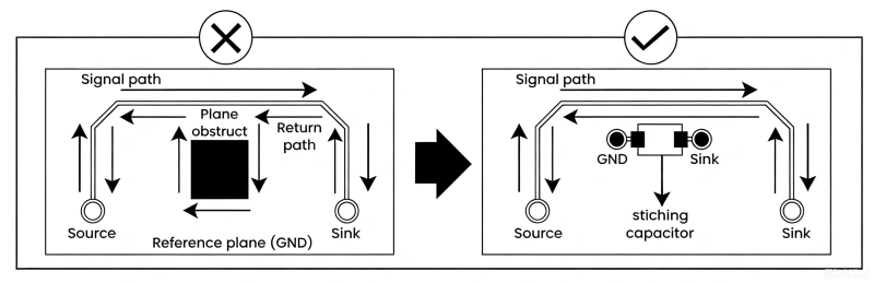
To lower electromagnetic emissions and boost immunity to external interference, engineers must deliberately design the physical path that the return current takes. Current will always take the path of least impedance. At frequencies above a few kilohertz, the path of least impedance is the path of least inductance, which naturally mirrors the signal trace itself.
Parallel Guard Traces on Single-Sided PCBs: On single-sided boards, there is no second copper layer to serve as a return reference. To combat this limitation, designers must route a dedicated ground wire directly alongside critical high-frequency signal lines. This guard trace should be positioned as close to the signal line as copper spacing tolerances allow.
This layout creates a highly localized, low-impedance loop. Instead of returning through a distant ground path, the signal current returns through the adjacent guard trace. This structure limits the loop area and isolates the sensitive signal from neighboring routing lines, preventing capacitive crosstalk.
Co-Planar and Under-Trace Grounding on Double-Sided PCBs: On double-sided boards, the optimal return path lies directly beneath the signal trace on the opposite layer. The loop area is then minimized to the product of the dielectric board thickness (H) and the trace length (L):
A = H × L
To execute this effectively:
For double-sided boards, laying down a dedicated ground grid (also known as a ground mesh) is an essential design standard to reduce ground loop impedance and improve overall PCB EMC performance. A ground grid is formed by routing a mesh of horizontal ground lines on one side of the board and vertical ground lines on the other, joining them with vias at every intersection.
The equivalent electrical impedance of a ground return path is determined by:
Zg = Rg + jωLg
Where:
At high frequencies, the reactive term (jωLg) dominates. By implementing a ground grid, we introduce multiple parallel ground paths, reducing the equivalent ground inductance (Lg) and keeping ground bounce to a minimum. Furthermore, the mesh pattern ensures that an adjacent return path is always available near any signal line, which drastically limits loop areas across the entire board. This technique is particularly important during professional turnkey PCB assembly services, as robust grounding prevents component-level interactions and signal degradation during high-speed switching.
To help designers select the optimal board stackup for their performance targets and budget, the table below compares key electrical and electromagnetic characteristics of single-sided, double-sided, and multilayer configurations.
| EMC Design Parameter | Single-Sided PCB | Double-Sided PCB (Standard) | Double-Sided PCB (With Ground Grid) | Multilayer PCB (4+ Layers) |
|---|---|---|---|---|
| Average Ground Impedance | Extremely High | High to Moderate | Low to Moderate | Extremely Low |
| Loop Area Control | Difficult (Requires Guard Traces) | Moderate (Requires Careful Routing) | Very Good | Excellent (Solid Plane Reference) |
| Differential-Mode Shielding | Poor | Moderate | Good | Excellent |
| Crosstalk Suppression | Very Low | Moderate | High | Exceptional |
| Relative Manufacturing Cost | 1.0 (Baseline) | 1.2 - 1.4 | 1.2 - 1.4 | 2.0 - 3.5+ |
While multilayer boards offer superior shielding, implementing a disciplined ground grid and parallel guard traces allows double-sided PCBs to achieve clean performance figures suitable for many consumer electronics. More detailed layout practices can be studied in our article on advanced PCB grounding techniques.
The loop area (A) of a trace on a double-sided PCB is approximately equal to the length of the signal trace (L) multiplied by the thickness of the dielectric core substrate (H), expressed as A = L × H. Minimizing both trace length and board thickness directly reduces the loop area.
A ground grid creates a dense, low-impedance mesh of copper pathways across the entire board. This layout ensures that a return path is always adjacent to any given signal line, significantly shrinking the loop area and preventing common-mode noise propagation that compromises EMC compatibility.
A ground guard trace should be placed as close to the high-speed signal trace as manufacturing tolerances and voltage safety margins allow, typically following the 3W spacing rule. This tight proximity forces the signal's return current to flow through the adjacent guard trace, minimizing the loop.
Yes, single-sided PCBs can meet strict international standards (like FCC or CE), but it requires highly disciplined routing. Designers must place parallel return traces alongside every high-frequency signal, maximize ground copper pours, and physically isolate sensitive analog components from noisy digital switching zones.
Differential-mode radiation is caused by signal currents flowing through loop areas on the PCB, which can be mitigated by reducing the loop size. Common-mode radiation is driven by high-frequency noise voltages driving external cables, which requires proper grounding, filtering, and shield termination to suppress.

Still, need help? Contact Us: support@nextpcb.com
Need a PCB or PCBA quote? Quote now

