Support Team
Feedback:
support@nextpcb.comIn the electronics manufacturing industry, PCB (Printed Circuit Board) as a carrier of circuits and devices, the advantages and disadvantages of its manufacturing process directly affects the quality and performance of the product. In the PCB manufacturing process, the positive and negative processes are two very different manufacturing methods, each with their own unique characteristics and applicable scenarios. Today, we will explore the differences between the PCB positive process and negative process to help you better understand the two manufacturing processes.

Positive process, also known as pattern process, the use of the liquid for alkaline etching.
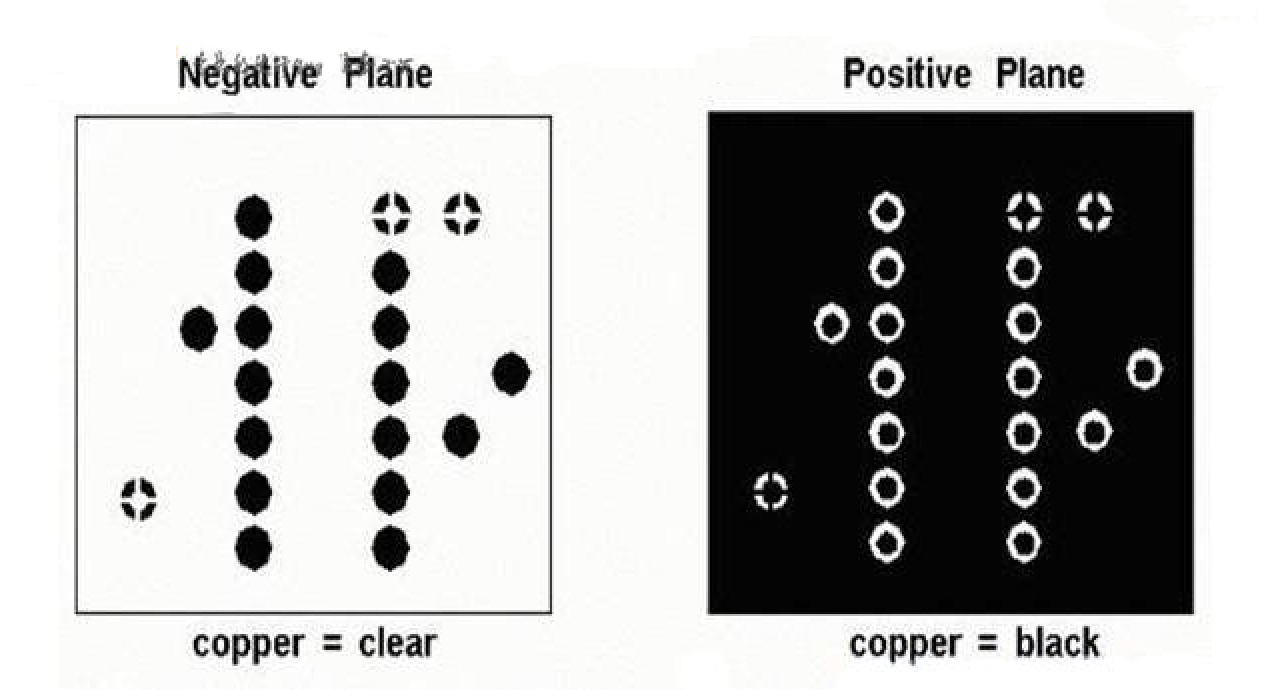
In the positive process, where the line is drawn (i.e., the line needs to be retained) the copper of the printed circuit board is retained, and no line is drawn (i.e., does not need to be wired in the region) the copper is removed. For example, the top and bottom signal layers are positive sheets.
Negative production: The lines or copper surfaces that need to be retained are black or brown, while the parts that do not need to be retained are transparent.
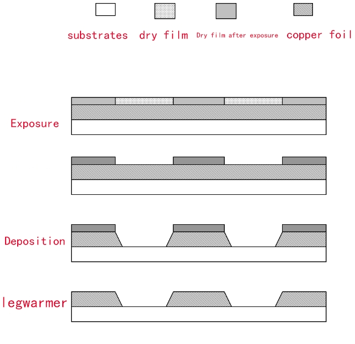
Line Process Exposure: The transparent portion is chemically hardened by light exposure to a dry film resist.
Developing process: The dry film that has not hardened is washed away.
Tin-lead plating process: Tin-lead is plated on the copper surface where the dry film has been washed off in the previous process (developing).
Deprocessing: Removal of dry film hardened by exposure to light.
Etching process: The copper foil without tin-lead protection (transparent part of the negative) is bitten off with an alkaline solution, and what remains is the desired line (black or brown part of the negative).

Positive: the process is (double-sided board) opening - drilling - PTH (a plating is also called thickened copper) - line - two copper (graphic plating) and then go to the SES line (depaneling - etching - retinning)
Less error rate, because the positive process uses the way to add dynamic copper, basically can meet all the design requirements.
It is more suitable for PCBs with high line width requirements. in the positive process, the lines are inverted trapezoidal, which helps to minimize the flying line problem (i.e., the phenomenon of the copper plating layer peeling off from the substrate).
Compared to the negative process, the positive process requires more complex graphic plating steps, which may increase the use of materials and resources.
Negative process, also known as tenting process, the use of the liquid for acid etching.
In the negative process, where the line is drawn (i.e., the need for wiring the region) of the printed circuit board copper is removed, no line is drawn (i.e., do not need to be wired in the region) copper is retained instead. The internal power/ground layer (referred to as the internal power layer) is usually used in the negative process to lay out the power and ground lines.
Negative Processing: The wiring or copper surfaces to be retained are transparent, while the unwanted portions are black or brown.
Line Process Exposure: The transparent portion is chemically hardened by the exposure of the dry film resist to light.
Developing process: The dry film that has not hardened is washed away.
Etching process: Only the part of the copper foil that has been washed out of the dry film (the part of the negative that is black or brown) is etched, leaving the part of the dry film that has not been washed out (i.e., the desired line, the transparent part of the negative).
De-filming: Removal of the remaining dry film, leaving the desired lines.
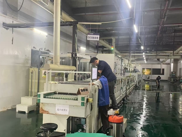
Negative: process is (double-sided panel) open material - drilling - PTH (a plating also known as thickened copper) - line (not after the two-copper graphic plating) and then go to the DES line (etching - de-filming)

The negative process is favored by many PCB manufacturers because of its low starting cost. This process eliminates the need for complex graphic plating steps, thus reducing material and resource usage.
The negative process is capable of etching line widths of 23 mil (5075 μm) at a copper thickness of 0.5 OZ, making it a cost-effective option for designs that do not require high line widths or are not too thick in copper.
The advantage of the negative process is that it defaults to a large copper fill, which eliminates the need to reset when adding vias, changing the size of the copper deposit, etc., and saves the time required to re-calculate the copper deposit.
The negative process may not perform as well as the positive process for fine line fabrication.
When using the negative process, it is necessary to more carefully specify which areas do not require copper, which may increase the design complexity.
| Aspect | Positive Process | Negative Process |
| Cost | Higher (complex plating steps) | Lower (simpler process) |
| Line Width | Supports finer lines | Suitable for thicker, less precise designs |
| Design Complexity | Relatively low (add copper incrementally) | Higher (define areas without copper) |
| Error Rate | Lower (dynamic copper addition) | Slightly higher |
| Application | High-end or fine-line products | Economical for general applications |
Still, need help? Contact Us: support@nextpcb.com
Need a PCB or PCBA quote? Quote now