
 NextPCB Capabilities
Printed Circuit Boards
NextPCB Capabilities
Printed Circuit Boards
 PCB Assembly
 Layer Buildup
 SMD-Stencils
 PCB Design-Aid & Layout
 Mechanics
 Quality
 Drills & Throughplating
 Factory & Certificate
 PCB Assembly Factory Show
Certificate
PCB Assembly Factory Show
Certificate
Support Team
Feedback:
support@nextpcb.com


This article is going to tell you about the PCB Advanced Spacing Rules on Altium designer.
For example, the copper pour pitch is 16mil, other safety pitches are 8mil, the via-to-via pitch is 100mil, the pad-to-pad pitch is 100mil, the pad-to-via pitch is 100mil, the top ground copper is 0.8mm, the top layer
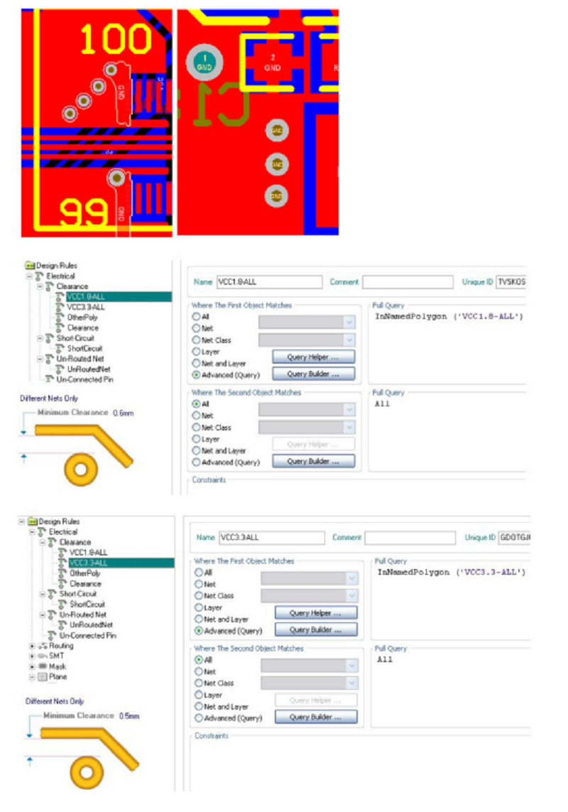
The distance between VCC3.3 and VCC1.8 is 0.5mm.
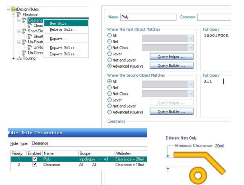
Altium Designer's spacing rules default to a 10mil spacing, and there is no distinction between pads to pads, vias to vias, and traces to copper. If you want advanced rules, you must create new ones yourself.
Under Design>Rules>Electrical>Clearance in the PCB design environment, right-click to create a new spacing rule and rename it to Poly, select Advanced (Query) for Where The First Object Matches, enter polygon for Full Query and change the default 10mil to 20mil for Constraints. The level Poly is higher than the default Clearance of 10mil. These two spacing rules together constitute a copper-clad spacing of 20mil. The spacing, such as routing to routing, and routing to pad vias, is a rule of 10mil, as shown in the following figure:
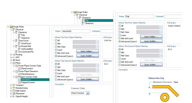
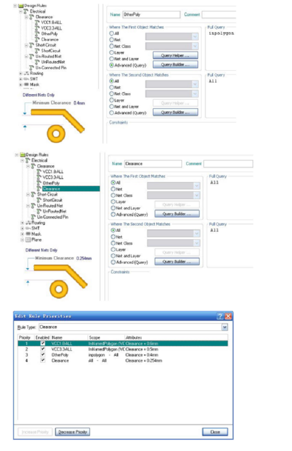
The following 2 figure shows the viaconnect with copper-clad full-connected vias, the default safety clearance is 8mil, and the copper-clad spacing is 16mil regular copper-clad. Inpolygon is all copper-clad. If you want other copper-clad spacing, you need to create a new copper-clad rule. For example, VCC3.3 copper pour 0.5mm, VCC1.8 copper pour pitch 0.6mm, other copper pour 0.4mm; priority 16mil is the lowest; pour a piece of copper to the VCC3.3 network and name the copper pour VCC3.3-ALL; Pour a piece of copper to the VCC1.8 network and name the copper-clad VCC1.8-ALL; the spacing rules must also be built, see the following pictures 3-6:
The following figure shows the spacing rules from via to via, Where The First Object Matches, Where The Second Object Matches FullQuery, only one of these two parameters is isvia and the other is ispad; if one is ispad and the other is isvia , That is the spacing between vias and pads; if one is ispad and the other is ispad, that is the spacing between pads and pads; then fill in the specific spacing, where The Second Object Matches defaults to ALL, modify it It is the first and second spacing rules, IsVia and ALL are the spacing rules from Via to other, IsVia and IsVia are the spacing rules from via to via;
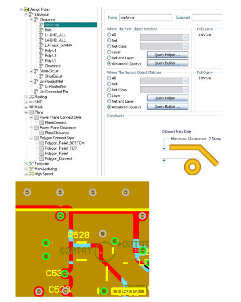
If the distance between vias and vias is not 2.54mm, the online DRC check shows a green display;
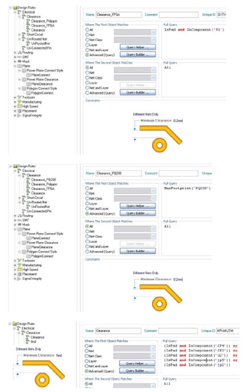
Note: Set the small-pitch pin pitch: some FPGA chips and many other pad pitches have reached 0.2mm. The default 10mil (0.254mm) pitch is obviously in conflict. The above problems can be passed
HasFootprint('PQ208') or IsPadandInComponent('U1'); (IsPadandInComponent('JP4'))or(IsPadandInComponent('JP3'))HasFootprint('PQ208'), packaged as a PQ208 component; spad and InComponent('U1 '), the spacing between the pins of component U1;
The above two rules are only the pin spacing. The spacing of the lines pulled out from the cluster is other rule values, of course it should not be too large; for example, the PQ208 pad above is 0.3mm. The distance between pads is 0.2mm, and the wiring is 0.5mm, the distance between the wires drawn out is 0.4mm. If the wiring spacing is set to 0.5mm, 1mm, it is either green or cannot be pulled out; (IsPad and InComponent('JP4')) or (IsPad and InComponent('JP3')), the spacing rules of components JP3, JP4; see The following 3 pictures:
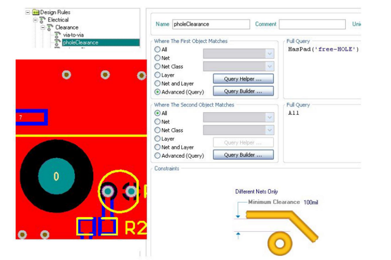
The following figure is a spacing rule with a positioning hole spacing of 3mm: a pad with an inner hole = an outer hole is often used as a positioning hole. The hole is not connected to any network (no electrical connection), only screws are used. We put 4 positioning holes on the 4 pins on the PCB, which are not connected to any network. The name of the pad starts from HOLE, inner hole = outer hole size; free-hole means free is not connected to any network, Hole pad name; It can be free-0, free-1, free-2, etc.;
The picture below shows a spacing rule named 5VANA on the toplayer layer with copper. Of course, toplayer can be replaced with other layers, and 5VANA can be replaced with other copper-clad names;

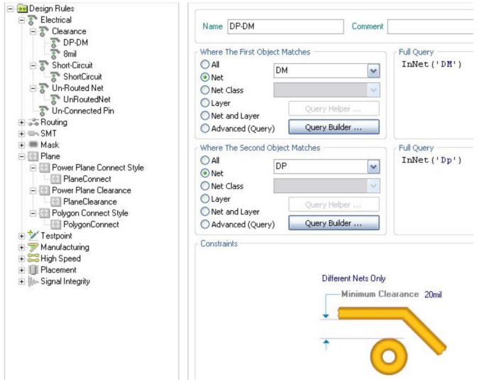
The following figure shows the distance rule from DM to DP network with a distance of 20mil:
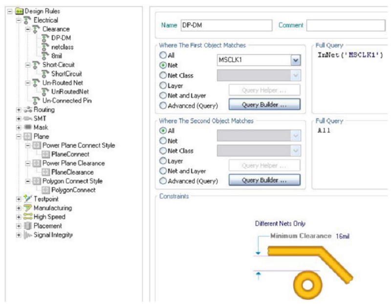
The following figure shows the spacing rules from MSCLK1 network to other 16mil spacing:
Still, need help? Contact Us: support@nextpcb.com
Need a PCB or PCBA quote? Quote now


 Surface


Susan
Using a well-defined set of design rules, you can successfully complete circuit board designs with different and often stringent design requirements. In addition, since the PCB editor is rule-driven, taking the time to set up the rules at the beginning of the design will enable you to effectively carry out the design work and know that the rule system is working hard to ensure success.