
 NextPCB Capabilities
Printed Circuit Boards
NextPCB Capabilities
Printed Circuit Boards
 PCB Assembly
 Layer Buildup
 SMD-Stencils
 PCB Design-Aid & Layout
 Mechanics
 Quality
 Drills & Throughplating
 Factory & Certificate
 PCB Assembly Factory Show
Certificate
PCB Assembly Factory Show
Certificate
Support Team
Feedback:
support@nextpcb.com


A single reversed diode in a schematic can ruin an entire PCBA run. Not because the component is wrong — but because the engineer who placed it didn't fully understand what the symbol was telling them.
Schematic symbols are not just icons. Behind every zig-zag resistor or triangle-and-bar diode is a chain of manufacturing decisions: which physical package gets ordered, how the netlist maps to copper traces, whether the BOM populates correctly at the assembly stage. Miss that chain, and a symbol error that takes seconds to spot in a schematic can cost days of rework on a physical board.
This guide covers the electrical and electronic symbols used in PCB design — not just what they look like, but what they mean for the real-world journey from schematic capture to PCBA delivery. You will learn how standardized symbols (IEC 60617 and ANSI/IEEE 315) protect your design across global supply chains, how each symbol's pin assignments link to physical footprints, and which symbol-related errors most commonly surface during DFM reviews.
If you are completely new to schematics, start here. If you are already designing boards and need a comprehensive visual lookup of 100+ symbols organized by category — diodes, MOSFETs, logic gates, ground types, and more — use our dedicated Visual Reference guide alongside this one.
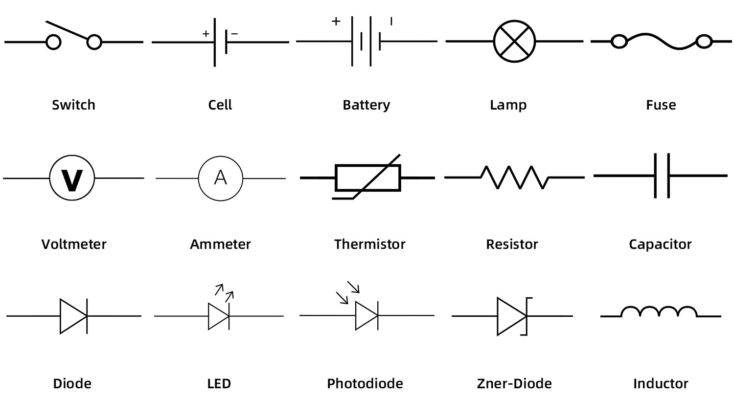
A visual depiction of electrical and electronic components is known as an electrical symbol. These symbols enable engineers to identify a specific electronic component within a complex schematic diagram. Electrical symbols utilize national and international standards (such as IEEE, ANSI, and IEC) for their precise definitions. It is important to note that while circuit symbols show the components and their logical connections, they do not inherently specify the physical size, footprint, or exact operational method—that information is managed by the component's metadata in the CAD software.
Circuit symbols represent each component in a circuit logically. Each component has a specific number of connections, referred to as pins or terminals. The schematic includes clear labeling for these pins. For example, in a turnkey PCB design workflow, a 3-pin transistor symbol in the schematic must perfectly map to the 3 pads of a SOT-23 physical footprint on the PCB layout.
One of the most fundamental parts of an electrical circuit diagram is an electric power source. A battery, for instance, features positive and negative terminals. The wires, representing copper traces on a bare board, connect the components. Junctions where wires connect are typically shown as solid blobs or dots (nodes), while crossing wires without dots imply no electrical connection.
A modern circuit diagram includes numerous active and passive components. Nets (logical wire connections) link them together. When sending a design to a PCB manufacturer, these logical nets are exported as a "Netlist," which guides the routing of the physical copper traces. Each element is also assigned a unique reference designator (e.g., R1 for a resistor, C1 for a capacitor) and value properties (size, voltage rating, wattage), which eventually populate the Bill of Materials (BOM) used for PCB assembly.
The technical definition of an electronic circuit is a grouping of different electronic parts that interact to manipulate the movement of an electric current for a specific functional outcome. To create a workable schematic diagram, the symbols representing these electrical components must have two or more terminals that are used to join one component to another.
In Electronic Design Automation (EDA) software like Altium Designer, KiCad, or Cadence Allegro, an electronic symbol is actually the graphical front-end of a complex database entry. Behind the simple zig-zag line of a resistor symbol lies critical data: the manufacturer part number (MPN), tolerance, package size (e.g., SMD 0402 or 0603), and 3D step models.
Basic symbols include ground planes, power rails, and passive components. By understanding these, you can map out highly complex architectures, such as microcontrollers interfacing with memory ICs and power management units. When building circuits for a prototype or moving directly to mass production, understanding these electronic symbols is non-negotiable. Without a flawless schematic, the subsequent PCB layout will be inherently flawed, leading to severe issues during PCBA.
Electronic circuit symbols act as the blueprint. Common symbols encompass switches, sources, ground nets, resistors, capacitors, diodes, inductors, logic gates, transistors, amplifiers, and transformers. These symbols establish the "Design Intent," which CAM (Computer-Aided Manufacturing) engineers at NextPCB review during the initial Design for Manufacturing (DFM) check.
Imagine the chaos if every hardware engineer invented their own symbols for common components. The primary reason we use a strict set of symbols is global interoperability. Another name for it is a schematic library standard.
According to its operating features, each component behaves in a specific manner. A connected route (trace) connects electronic components in an electronic circuit to complete the circuit path. Most symbol designs are based on stringent national and international standards established decades ago but continuously updated. Prominent examples include:
When you utilize a quick turn PCB service, your files might be generated in the US and manufactured in Asia. Standardized symbols ensure that a polarized component, like a tantalum capacitor, is oriented correctly on the assembly line, preventing catastrophic failures like capacitor explosions upon initial power-up. While symbols represent individual parts logically, it is the engineer's responsibility to pair the correct symbol with the appropriate physical footprint (e.g., IPC-7351 standard footprints) for the assembled printed circuit board.
Electronic symbols simplify the drafting process, but their true value shines in the manufacturing phase. A symbol's precise meaning is conveyed through dots, lines, letters, shading, and pin numbers. Mastering these structural nuances is essential for anyone involved in hardware design or procurement.
These symbols communicate vital information about logical wiring and equipment interfaces, laying the groundwork for physical component placement on the PCB.

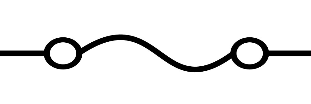
In electrical applications, the switch acts as the primary control mechanism. Its core purpose is to transition a circuit between an "open" (current interrupted) and "closed" (current flowing) state. In PCB layout, switches require careful footprint design to withstand mechanical stress from user interaction.
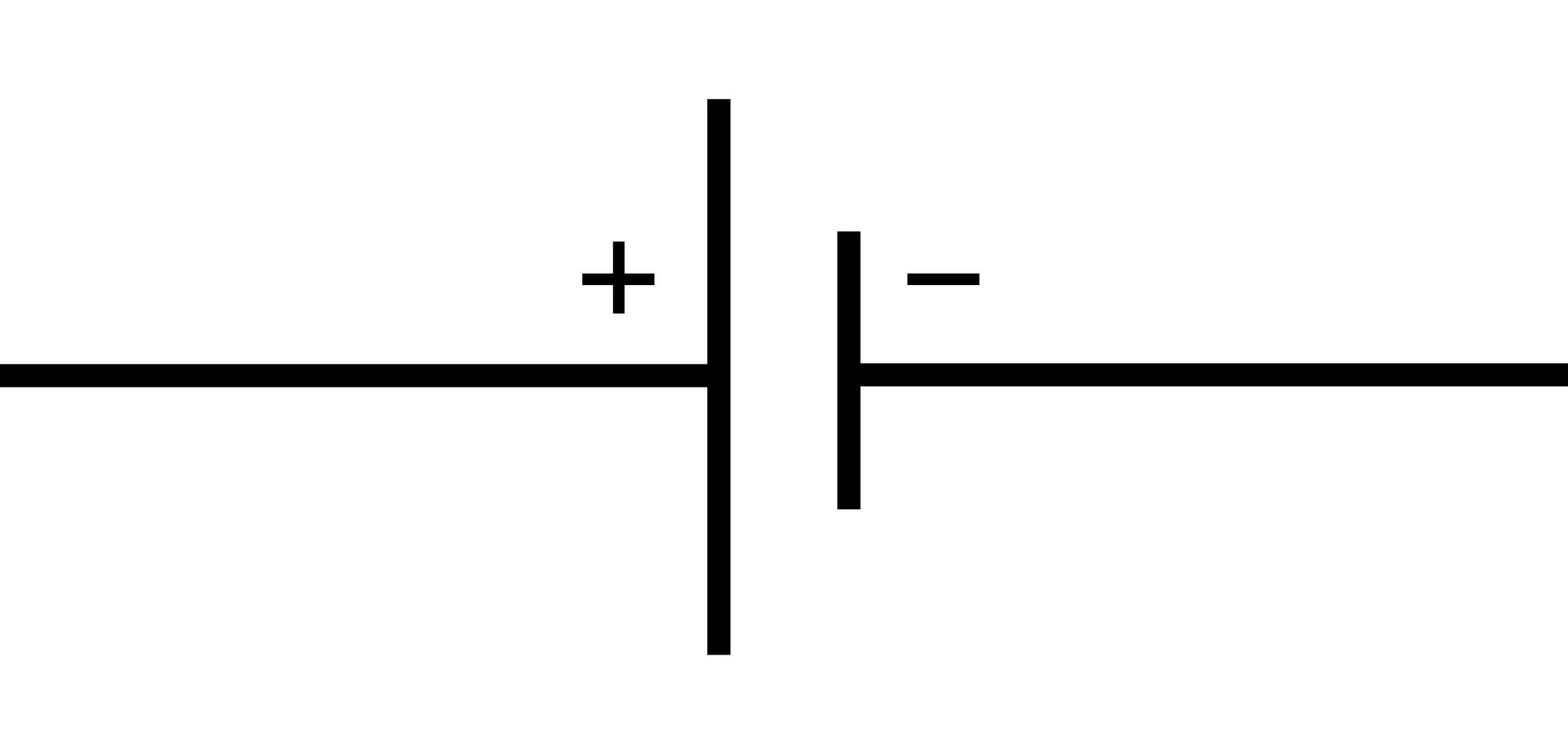
The electrical cell is the fundamental unit that provides the potential difference (voltage) to power the circuit. It represents a single unit of chemical-to-electrical energy conversion. The longer line in the symbol represents the positive terminal (anode), while the shorter, thicker line represents the negative terminal (cathode).
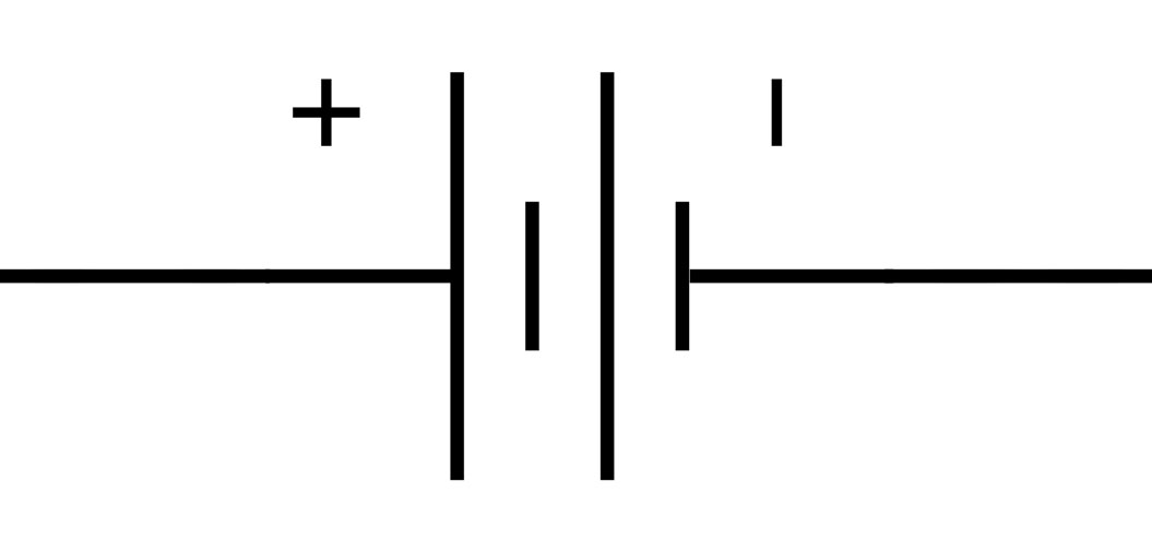
A battery is simply two or more cells connected in series or parallel to increase voltage or capacity. In modern PCB design, accommodating batteries often means designing footprints for SMD coin cell holders (like the CR2032) or incorporating battery management system (BMS) ICs into the PCBA to handle lithium-polymer charging safely.
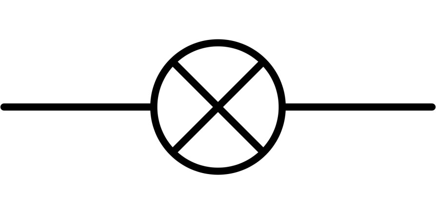
Historically representing an incandescent light bulb where current heats a thin filament, this symbol is less common in modern low-voltage PCBA, having been largely replaced by the LED. However, it still appears in schematics dealing with high-voltage AC load switching via relays or TRIACs.
A critical safety component. Traditional glass fuses contain a wire with a specific melting point that burns out during an overcurrent event, breaking the circuit. In contemporary turnkey PCB assemblies, designers often use Surface Mount (SMD) PTC resettable fuses (PolySwitch) which automatically reset once the fault condition is removed, significantly improving product longevity.
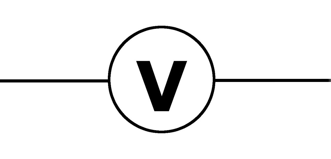
A voltmeter measures the electrical potential difference between two points in a circuit. It is always connected in parallel with the component being measured. While mostly an external diagnostic tool, in automated PCBA testing (like Flying Probe or Bed of Nails testing), specific test points are designed directly into the PCB layout so robotic voltmeters can verify board functionality post-production.
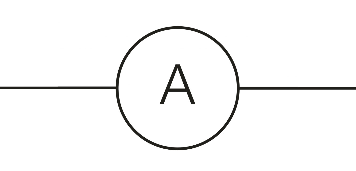
An ammeter measures electric current and is always placed in series with the circuit path. In modern embedded PCB designs, actual ammeter components are rare; instead, engineers use precise, low-value "shunt resistors" combined with current-sense amplifier ICs to actively monitor power consumption directly on the board.
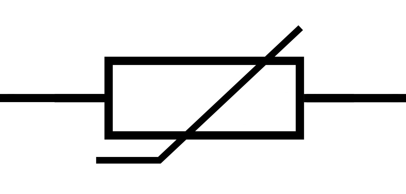
Thermistors are temperature-dependent resistors. NTC (Negative Temperature Coefficient) thermistors reduce resistance as temperature rises, while PTC (Positive Temperature Coefficient) thermistors increase resistance. They are crucial in high-density PCB designs for thermal management, feeding temperature data to microcontrollers that can throttle CPU speeds or activate cooling fans to prevent the PCB from overheating.
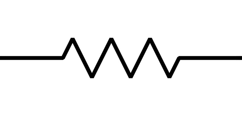
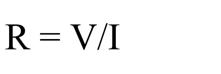
The resistor is the most ubiquitous passive component, designed to limit or regulate the flow of electrical current. There are two common symbols: the ANSI zig-zag line (common in the US) and the IEC simple rectangle (common in Europe). Resistance is measured in Ohms (Ω), defined by Ohm's Law (V = I * R).
From a PCB manufacturing standpoint, the schematic symbol must dictate the wattage and size. Modern low-cost PCBA relies heavily on miniature Surface Mount Device (SMD) resistors. Packages like 0603, 0402, and even microscopic 0201 or 01005 are standard. Selecting the right size is a critical DFM step; too small, and the resistor might exceed its power rating and burn; too large, and it wastes valuable PCB real estate.
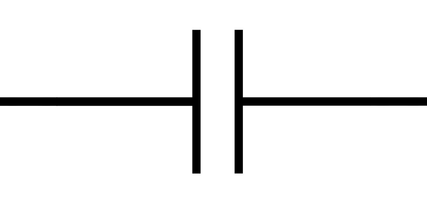
Capacitors store and release electrical energy, filtering noise and stabilizing voltage. They are absolutely critical as "bypass" or "decoupling" capacitors placed adjacent to every IC's power pin on a printed circuit board.
The symbol usually features two parallel lines. Crucially, there is a distinction between non-polarized capacitors (like MLCCs - Multi-Layer Ceramic Capacitors, which can be placed in any direction) and polarized capacitors (like Electrolytic or Tantalum). Polarized symbols feature a curved line or a "+" sign. DFM Warning: Reversing a polarized capacitor during PCB layout is a common error that leads to component explosion during the PCBA reflow or testing phase. Always ensure the schematic polarity matches the footprint's silkscreen.
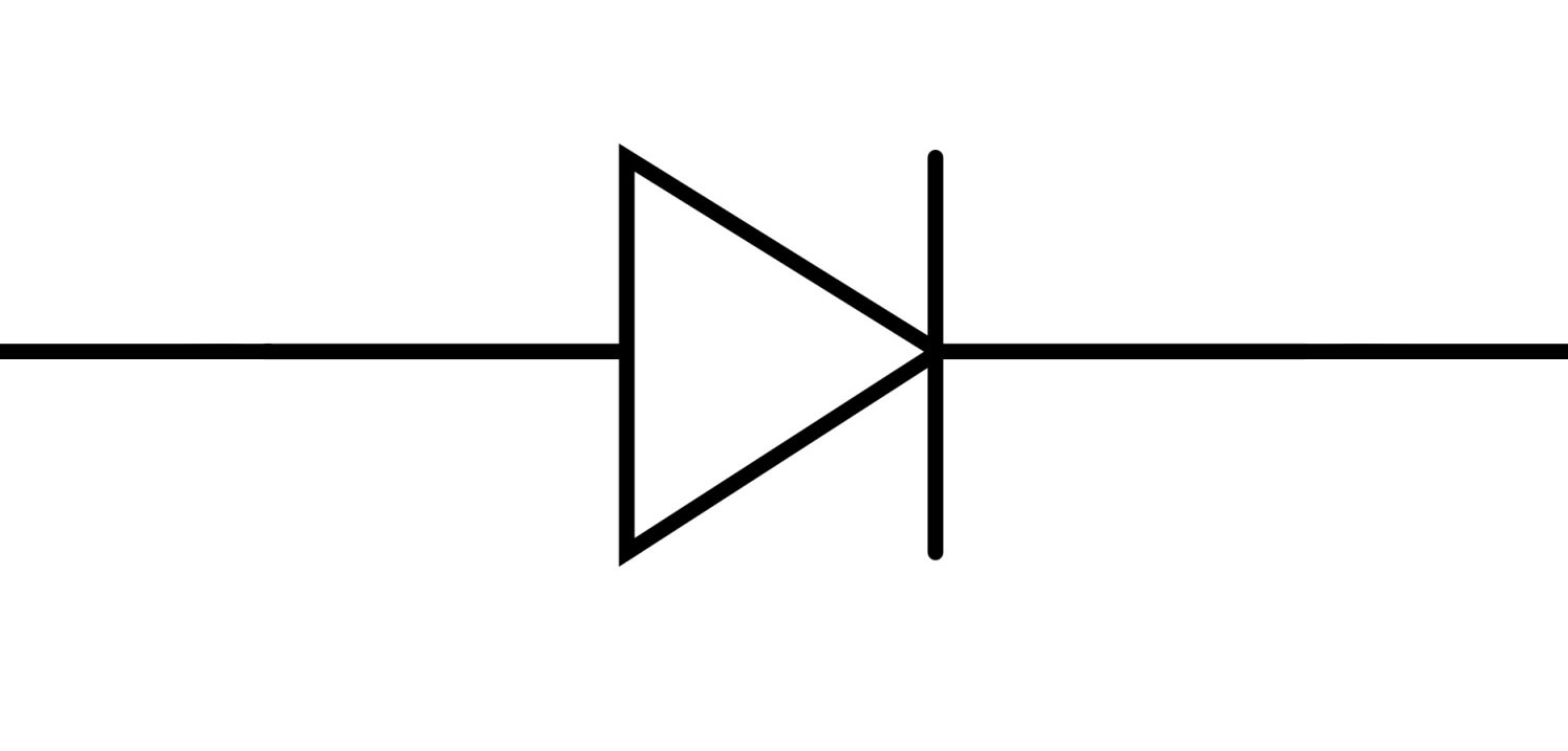
A diode is the electronic equivalent of a one-way valve for current. It permits current to flow from the Anode to the Cathode while blocking reverse flow. The symbol is a triangle pointing toward a straight line. The line represents the Cathode (negative).
In PCB layout, diodes are heavily polarized. The physical footprint will typically have a visible line or dot on the silkscreen layer denoting the cathode. If the schematic symbol pin assignment is flipped relative to the physical footprint, the PCBA will fail completely. Diodes are essential for reverse-polarity protection in power supply inputs.
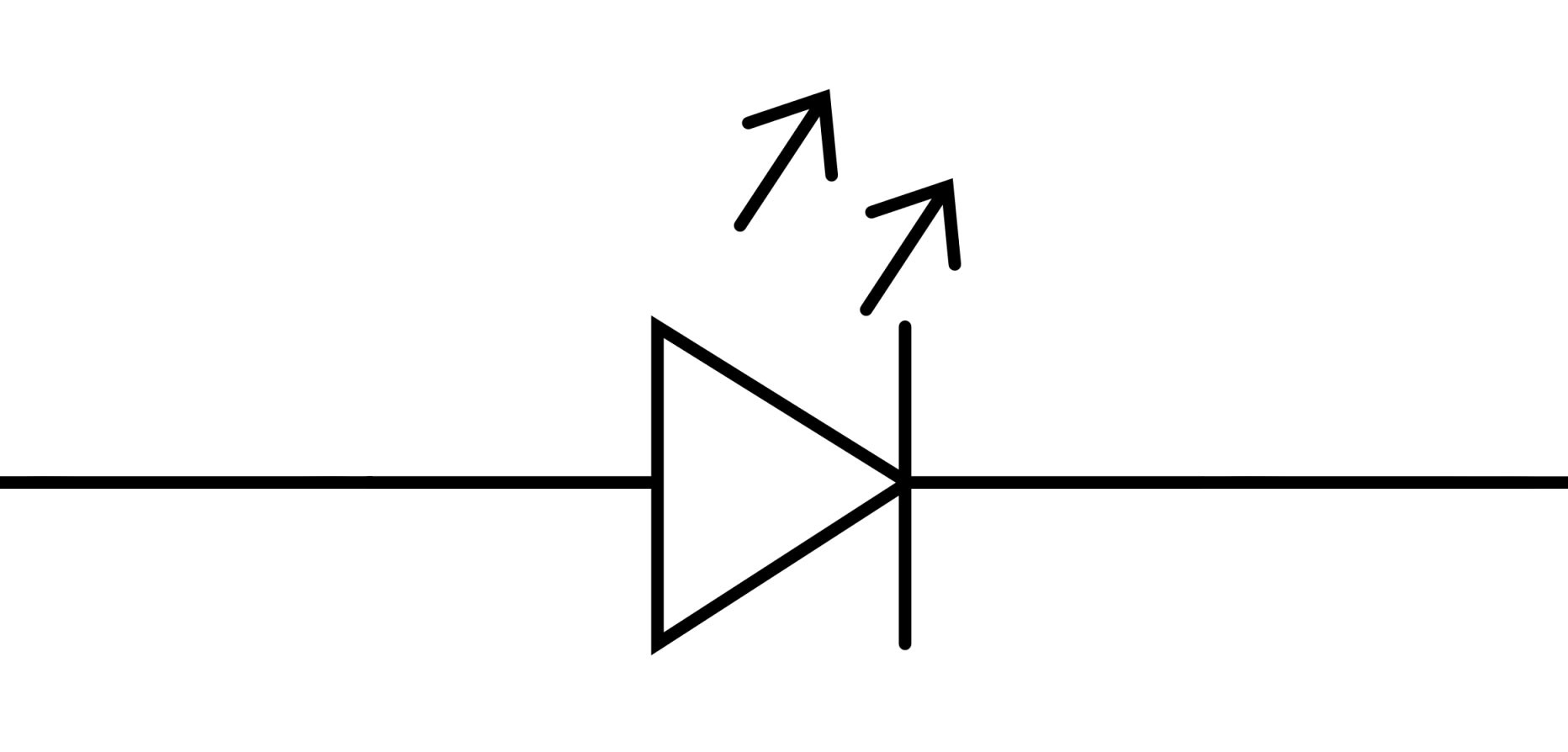
The LED symbol modifies the standard diode symbol by adding tiny arrows pointing away from the triangle, representing the emission of photons (light). Because LEDs are diodes, they are strictly polarized. High-power LEDs used in modern lighting circuits generate substantial heat; therefore, the PCB layout must incorporate thermal vias and copper pours beneath the component to dissipate heat, ensuring longevity.
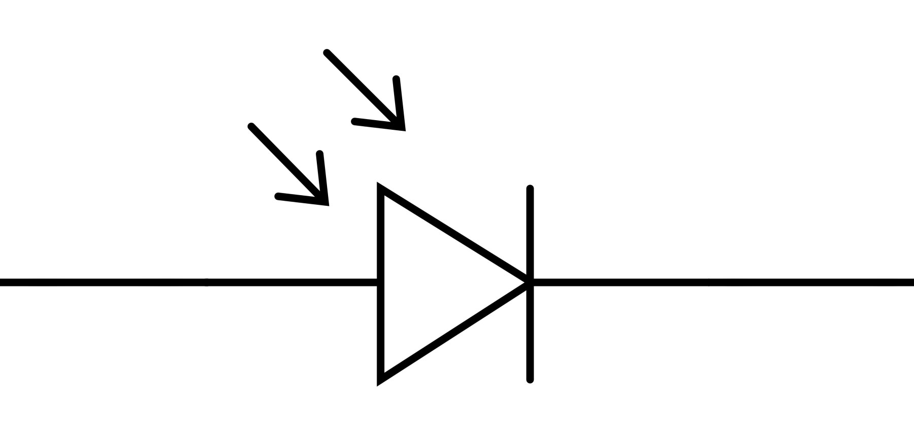
The photodiode symbol features arrows pointing towards the diode structure, symbolizing incoming light (photons) hitting the PN junction. They convert light into electrical current and are used in optical communication, ambient light sensors, and medical devices. Layout considerations include keeping analog traces short and shielded from digital noise to maintain signal integrity.
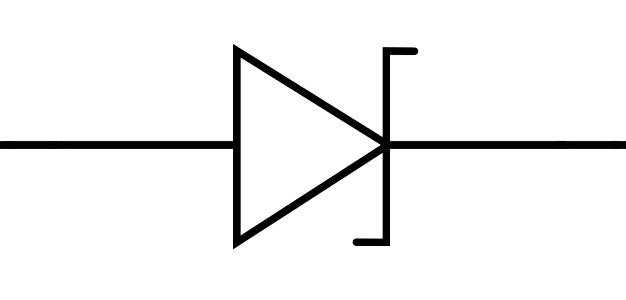
Unlike standard diodes that block reverse current entirely (until catastrophic failure), Zener diodes are intentionally designed to allow current to flow backward in a controlled manner once a specific "Zener breakdown voltage" is reached. The symbol features small "wings" on the cathode line. They are incredibly useful for simple voltage regulation and clamping voltage spikes to protect sensitive ICs downstream on the PCB.

An inductor stores energy in a magnetic field when current flows through it. The symbol depicts a series of loopy coils (ANSI) or a filled black rectangle (IEC). Inductors oppose changes in current.
In modern PCB design, inductors are the heart of Switched-Mode Power Supplies (SMPS), enabling efficient step-up (boost) or step-down (buck) voltage conversion. Because inductors generate magnetic fields, PCB placement is a high-level DFM concern. They must be placed carefully to avoid Electro-Magnetic Interference (EMI) from coupling into sensitive analog traces or antennas nearby.
Understanding symbols is only half the battle. In a professional hardware development cycle, the schematic is captured and then verified using a Design Rule Check (DRC). This automated process ensures no logical rules have been broken (e.g., outputs shorted together, floating pins).
Once the schematic is clean, it generates a Netlist. The Netlist is the bridge that tells the PCB layout software exactly which physical footprints need to be connected by copper traces. If a symbol in the schematic has an incorrect pin mapping (e.g., Pin 1 of the schematic symbol connects to the Base of a transistor, but Pin 1 on the physical footprint connects to the Emitter), the final PCBA will be fundamentally broken, regardless of how perfectly the manufacturer fabricates the bare board.
Choosing an experienced EMS partner is vital. At NextPCB, our engineering team performs rigorous preliminary DFM reviews on your Gerber files, BOM, and pick-and-place data, acting as a second line of defense against schematic-to-layout discrepancies before manufacturing begins.
While often used interchangeably, electrical symbols typically represent macroscopic power, electromechanical, and safety devices (switches, relays, motors, fuses, high-voltage transformers). Electronic symbols represent smaller, mostly semiconductor-based components used to manipulate low-voltage signals and logic (transistors, ICs, diodes, microcontrollers).
Generally, bare-board PCB manufacturers only need your Gerber files (physical layout) and do not review the schematic. However, if you are using a turnkey PCBA service like NextPCB, our CAM engineers cross-reference your BOM (Bill of Materials), Centroid (Pick and Place) files, and physical footprints to ensure polarities and package sizes align perfectly, preventing costly assembly errors.
If a polarized component (like a Tantalum capacitor, Diode, or IC) is connected backward due to a schematic error or footprint mismatch, the component will fail to function. In the case of polarized capacitors or power regulators, applying reverse voltage will frequently cause the component to overheat, vent, or explosively fail, potentially ruining the entire Printed Circuit Board.
There is no single global standard, but the IEC 60617 standard is the most dominant internationally, particularly in Europe and Asia. In the United States, ANSI/IEEE 315 remains prevalent. Most modern EDA software allows engineers to seamlessly toggle between standard libraries based on their client's geographic location.
You must consult the component manufacturer's datasheet. The datasheet will specify the exact land pattern (footprint) required, usually referencing the IPC-7351 standard. Your EDA software library links the logical symbol pins to the physical footprint pads. Always verify this linkage before generating manufacturing files for a low cost PCB run.
Electronic and electrical symbols are the absolute foundation of hardware engineering. They are not mere drawings; they are data-rich signifiers that dictate the logic, part selection, and physical layout of a printed circuit board. Recognizing the nuances between different standards (ANSI vs. IEC) and understanding how a symbol's polarity or terminal configuration translates to a physical SMD or THT package is what separates an amateur from a professional hardware designer.
As components shrink and circuit density increases, the margin for error from schematic capture to PCB layout approaches zero. Whether you are laying out a simple power supply or a complex multi-layer high-frequency telecom board, rigorous adherence to standardized symbols ensures that your design intent is perfectly preserved throughout the manufacturing pipeline.
By mastering these symbols and their real-world manufacturing implications, you eliminate the risk of layout failures, streamline your BOM generation, and ensure smooth communication with your fabrication partners.
Ready to turn your perfect schematic into reality? Transitioning from CAD to physical hardware requires a reliable partner. NextPCB offers industry-leading turnkey PCB manufacturing and PCBA services. From rapid prototyping and quick turn PCB fabrication to mass production, our intelligent DFM systems and expert engineering teams ensure your designs are built exactly to your specifications, with zero compromises on quality. Contact NextPCB today to quote your next hardware project.
Still, need help? Contact Us: support@nextpcb.com
Need a PCB or PCBA quote? Quote now


 Surface

