
 NextPCB Capabilities
Printed Circuit Boards
NextPCB Capabilities
Printed Circuit Boards
 PCB Assembly
 Layer Buildup
 SMD-Stencils
 PCB Design-Aid & Layout
 Mechanics
 Quality
 Drills & Throughplating
 Factory & Certificate
 PCB Assembly Factory Show
Certificate
PCB Assembly Factory Show
Certificate
Support Team
Feedback:
support@nextpcb.com


We often use abbreviations and acronyms, especially in the electronics design and circuit board manufacturing sectors; hence, knowing and understanding these acronyms is essential. Among the terms used most frequently in the fabrication of electrical devices are PWB and PCB. These two definitions have even given rise to discourse, as these terms are sometimes interchangeable within the electronics industry.
In this article, we will cover how to differentiate PWB from PCB. As these terms can be confusing, it is essential to know them both. Read along as we discuss the similarities and distinctions between the two to help address the questions you may have about PWB and PCB.
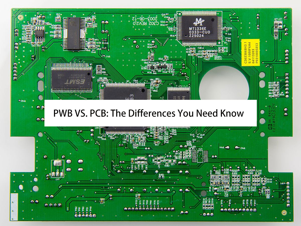
PWB and PCB stand for Printed Wiring Board and Printed Circuit Board, respectively. These terms refer to the board that provides the physical support and electrical connections for electronic components. While they are both common in electrical and electronic devices, they have distinct differences. Let us break down some key areas to further grasp these overlaps and differences.
One key difference between PWB and PCB is the technology fabricators employ in the assembly process.
PWB refers to a board without circuitry in an electronic device, utilizing an epoxy glass substrate without any printed components. It is an earlier technology, where in order to provide conduction-insulating surfaces between conduction-enabling traces, they etch the materials during the production process to create connections. It involves manually drawing and etching circuits onto the board and attaching components from point to point, in accordance with a specified design, resulting in an electronic circuit that can be used to create electronic devices.
On the other hand, PCB technology is more advanced and involves using a computer to design and create circuits on the board. PCB fabrication typically employs an insulating board with interconnected wires. Elements are then printed in a predefined design from point to point on a dielectric substrate. The size and spacing of the conductors profoundly affect how the circuit operates more than simply a point-to-point connection.
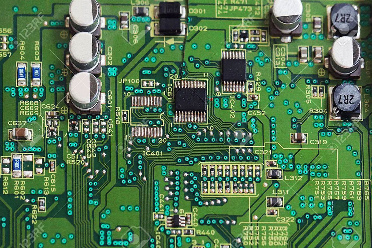
Key point: PCBs can be more complex and densely packed with components than PWB assembly. It is composed of elements connected by conductive tracks, pads, and other features etched from copper sheets laminated onto a non-conductive substrate.
PCB and PWB consist of various components in different materials. Due to the similarities in their designs, you may also find similar materials, which include conductive and non-conductive layers. Typically, the conductive layer aids signal transmission, while the non-conductive layer functions for electrical isolation. But then, it's worth noting that the materials to fabricate PWBs and PCBs are highly varied, depending on the application.
Copper, silver, and gold are popular PCB materials to provide a signal transmission channel for the conductive layer. While gold has the best conductivity with the least resistance, its inflated cost limits its application. Copper is favorable for most PWB and PCB applications as it is more economical with strong conductivity, among other advantages. The copper tracks can be applied directly onto the board by a process known as 'etching', or pre-made copper foil strips can be stuck onto the board.
A low-conductivity substance makes up the non-conductive layer. This layer usually utilizes FR-4, a composite epoxy material, and ceramic. Manufacturers commonly use FR-4 in a range of variations to improve its dielectric performance. Ceramic design substrates, on the other hand, are ideal for high-power applications due to their increased heat conductivity rate.
The prepreg substance is another typical material in PWBs and PCBs. The prepreg keeps the layers together, like the board core. Fabricators use resin-impregnated fiberglass, wherein when heated, it softens and binds to the layer surfaces before hardening and reinforcing a bond when cooled, which also helps to reduce vibration and shock damage.
Manufacturers also utilize materials like solder on these circuit boards. Solder is a substance composed of tin and lead, that manufacturers often use in component attachment to help preserve the copper from oxidation.
The conductive traces may be coated to avoid corrosion using materials like gold, nickel, silver, and tin, providing additional protection from dust and moisture.
Key point: There are many different materials that manufacturers use in the fabrication of PWBs and PCBs, offering varying degrees of insulation and heat conductivity, but common elements include fiberglass or plastic, along with copper tracks for electrical pathways, adhesive for holding components together, and a protective coating for dust and moisture resistance. The choice of material depends on the intended use of the board and the requirements of the electronic components it will support.
PWB serves as a foundation and framework for components that are wired together manually or with cables. It can involve soldering, crimping, splicing, or other wiring methods. As it allows you to move and re-route the wires over time, it is easy to make changes to the design without replacing the entire board. Hence, PWBs are preferable in projects where flexibility is a crucial factor.
On the other hand, PCB architecture employs automated processes like etching and plating. The components are mounted directly onto the board instead of being wired separately, allowing for more significant numbers of components to be connected in a much smaller space than what would be possible with PWB. This makes them more reliable because there's no need to worry about loose connections due to wear and tear over time. However, making changes to a PCB design requires completely replacing the board since all the components are embedded into it permanently. PCBs are suitable for projects that require high accuracy and repeatability, with minimal maintenance needed over time.
Key point: PCBs are considerably more advanced and versatile than PWBs due to their ability to support more complex circuits and a wider range of components.
Generally, PCB encompasses the entire circuits on a board, while PWB refers to the board itself. The distinction between the two is subtle, to the point that there is no official "correct" terminology.
Geography also plays a role in term usage. In the US electronics sector, the terms PCB and PWB are often interchangeable. PWB is an earlier term for boards in the early days of the tech industry. Eventually, the term came to characterize the functions of circuit architecture. While the term PCB is common in the prevailing US electronics sector, modern Japan adopts the term PWB. PCB was more prevalent when the technology sector initially emerged in Japan. However, because PCB also stands for "polychlorinated biphenyls," or poison, the term PWB has become preferable. Hence, both terms occur regularly in documents and articles from various periods and locations.
Aside from PCB and PWB, you may also want to be familiar with PCBA (Printed Circuit Board Assembly), CCA, PCA, and PWA. These are also terminology for printed circuit boards.
In the consumer electronics sector, the terms PWB and PCB are sometimes interchangeable. Printed wiring boards (PWBs) and printed circuit boards (PCBs) are both types of electronic circuits that are used to support and connect electronic components. They are integral parts of any electronic device; however, they serve different purposes when it comes to completing the circuitry.
In summary, the use of the term varies widely per region, but the fundamental distinction between the terms lies within the circuitry. PCBs contain pre-etched circuits, which allow them to be mass-produced quickly and efficiently; in contrast, PWBs have none. Generally, the printed wiring board is a fundamental step in PCB production. The intricate circuit boards we know today were originally PWBs; only they have now evolved to the point where the term PCB is now requisite. This breakthrough brought several benefits for PCB manufacturing in technology and research; however, it did not effectively wipe out the term PWB, which is the reason why both terms are still in use today.
Still, need help? Contact Us: support@nextpcb.com
Need a PCB or PCBA quote? Quote now


 Surface

