
 NextPCB Capabilities
Printed Circuit Boards
NextPCB Capabilities
Printed Circuit Boards
 PCB Assembly
 Layer Buildup
 SMD-Stencils
 PCB Design-Aid & Layout
 Mechanics
 Quality
 Drills & Throughplating
 Factory & Certificate
 PCB Assembly Factory Show
Certificate
PCB Assembly Factory Show
Certificate
Support Team
Feedback:
support@nextpcb.com


Addressing signal loss in PCB design is crucial for maintaining the performance and reliability of electronic systems. Considering the effects of signal loss during the design phase can help mitigate potential issues and ensure optimal system operation.
To minimize the signal loss in PCB design and ensure optimal performance and reliability of electronic systems, designers must focus on several key aspects. These include selecting appropriate materials, optimizing trace routing and length, maintaining impedance control, and employing proper termination techniques.
By paying attention to these factors, signal loss can be mitigated, particularly in high-speed and high-frequency applications.
This article provides a detailed understanding of signal loss in PCB design, including its causes, effects, and solutions.
PCB signal loss is a phenomenon that occurs when an electrical signal traveling through a Printed Circuit Board (PCB) experiences a degradation in strength and quality as it propagates through the circuitry. The signal loss can be caused by several factors such as conductor resistance, dielectric losses, and radiation losses.
PCB signal losses can result in a decrease in signal quality, slower transmission speeds, and ultimately, reduced performance of the electronic device. To mitigate signal loss, PCB designers and manufacturers implement various techniques such as impedance matching, controlled dielectric constants, and using higher quality materials.
Signal loss in PCB is one of the crucial factors to consider while designing the PCB. There are various types of signal loss in PCBs:
Insertion Loss: This is the decrease in signal power as it propagates through a component, connector, or PCB trace. It is typically measured in decibels (dB) and represents the difference between the signal's input and output power. Higher insertion loss indicates more significant signal degradation.
Attenuation: Attenuation refers to the gradual reduction in signal strength as it travels through the PCB. Resistive losses, capacitive losses, and skin effects cause it. Attenuation is also measured in decibels (dB). And it is directly proportional to the trace length and frequency of the signal.
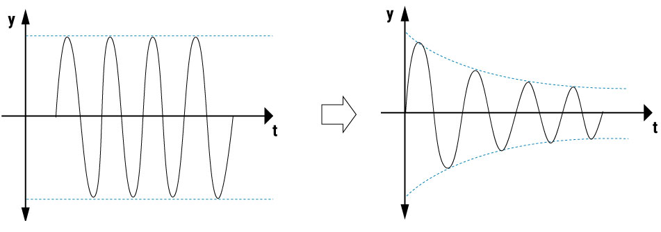
Reflection: Signal Reflection occurs when a portion of the signal is reflected toward its source due to impedance mismatches at the junctions between different transmission lines or components. Reflections can cause signal distortions, standing waves, and reduced signal integrity, especially at high frequencies.
Crosstalk: Crosstalk is the unwanted coupling of signals between adjacent conductive traces or components on a PCB. It can result from capacitive or inductive coupling. Besides, it causes interference, signal degradation, or even erroneous operation in electronic systems. Careful routing, shielding, and proper impedance matching can help minimize crosstalk.
Dielectric Loss: Dielectric loss is the attenuation of the signal due to energy absorption by the dielectric material used in the PCB. The extent of dielectric loss depends on the properties of the dielectric material, such as its dissipation factor and dielectric constant. Choosing low-loss dielectric materials and optimizing PCB stack-up can help minimize dielectric loss.
Various factors affect signal loss in PCB. Some of the common causes of signal loss include:
Conductor resistance: The inherent resistance of the conductive traces on a PCB can result in signal loss. As the signal travels along the trace, energy is dissipated as heat, leading to a weaker signal.
Impedance mismatch: Impedance mismatches between the source, transmission line, and load can cause signal reflections. It can lead to signal degradation, distortion, and loss of energy. Proper impedance matching and termination techniques help minimize signal reflections and associated losses.
Proximity effect: At high frequencies, the signal tends to travel near the surface (skin) of the conductive traces rather than penetrating deeper. This increases the effective resistance of the trace, resulting in a greater loss at higher frequencies. The proximity effect is a similar phenomenon where current density increases in conductors that are close together, leading to increased resistance and signal loss.
Substrate's dielectric properties: The dielectric materials used in PCBs can contribute to the loss. As the signal travels through the dielectric material, a small amount of energy is absorbed, causing attenuation. The choice of substrate material and its properties, such as dielectric constant and loss tangent, can impact signal loss.
Poor Material Quality: Poor quality materials can significantly impact the performance of a PCB by contributing to signal loss, noise, and other issues. Two primary materials in a PCB are conductive materials, such as copper traces, and dielectric materials, which separate conductive layers and traces.
Signal loss in PCBs can result in several negative impacts on the performance of electronic systems. These consequences include:
Distortion and attenuation: As the signal moves through the PCB, its amplitude, phase, or form may be altered due to resistance, capacitance, and inductance. This can cause the signal to become distorted and weakened, making it hard for the receiving end to interpret the transmitted data accurately.
Jitter and noise: Signal loss can cause jitter (timing fluctuations) and noise (unwanted signals) to be introduced into the transmitted signal. These factors can further degrade signal integrity and make it difficult for the receiver to extract the original information. In analog circuits, noise can reduce the signal-to-noise ratio (SNR), negatively impacting measurements' overall performance and accuracy or signal processing.
Higher bit error rates: PCB loss can result in higher bit error rates (BER), representing the proportion of incorrect bits compared to the total number of transmitted bits. Higher BER can cause data corruption and negatively impact system performance and reliability.
Crosstalk and interference: PCB loss can result in crosstalk, the undesired coupling of signals between adjacent conductive traces or components on a PCB. Crosstalk and interference issues can cause performance degradation in multiple aspects of a PCB.
EMI: Electromagnetic interference (EMI) can result from poor grounding, insufficient shielding, or inadequate trace separation, affecting the performance of sensitive components and potentially leading to system errors or failure.
Impacts on high-speed and high-frequency designs: Signal loss is particularly detrimental to high-speed and high-frequency strategies. It can cause significant signal integrity issues, making achieving the desired system performance difficult. In these designs, engineers must pay special attention.
Signal loss is a significant challenge in PCB design that can result in degraded signal quality and reduced performance. Here are some ways to mitigate signal loss in PCB design:
Controlled impedance design: When designing a controlled impedance PCB, consider factors such as trace width, thickness, dielectric constant, and trace separation from the ground plane. Use impedance calculators or simulation tools to verify that the design meets the desired impedance targets. Controlled impedance design helps to maintain signal integrity across the entire signal path, reducing the likelihood of signal distortion and reflections.
Proper material selection: The substrate material should have a stable dielectric constant and low-loss tangent across various frequencies. High-performance substrates such as Rogers or Isola materials may be required for high-frequency or high-speed designs. High-quality copper with a smooth surface finish for conductors will minimize resistance and loss. Electroless nickel immersion gold (ENIG) or immersion silver (ImAg) surface finishes can provide additional signal integrity and performance benefits.
Optimized trace geometry and routing: Use curved traces instead of sharp 90-degree angles to reduce impedance discontinuities and signal reflections. Implement techniques such as necking down or teardrops for pad-to-trace transitions to improve manufacturability and reliability. Avoid routing signals over slots or gaps in the ground plane, as this can introduce unwanted impedance changes and loss.
Proper use of termination techniques: Termination techniques are used to match the impedance of the transmission line to the load, reducing reflections and loss. Different termination methods are suitable for various applications and signal types. Place termination resistors close to the driver and receiver to reduce the length of unterminated stubs.
The performance of a PCB is heavily influenced by the signal integrity maintained within it. Careful consideration of design factors is essential when working with your solutions provider. Evaluating your PCB design against known risks can help ensure optimal performance and prevent issues from signal loss.
NextPCB is the one-stop solution for all of your high-quality PCB boards and assembly services. Experience a seamless journey from prototype to production with our quick turnaround times, competitive pricing, and superior quality. Feel free to contact us at any time. And you can request a quote if you want to know more about our services.
Still, need help? Contact Us: support@nextpcb.com
Need a PCB or PCBA quote? Quote now


 Surface

