

 NextPCB Capabilities
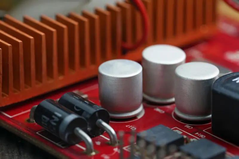
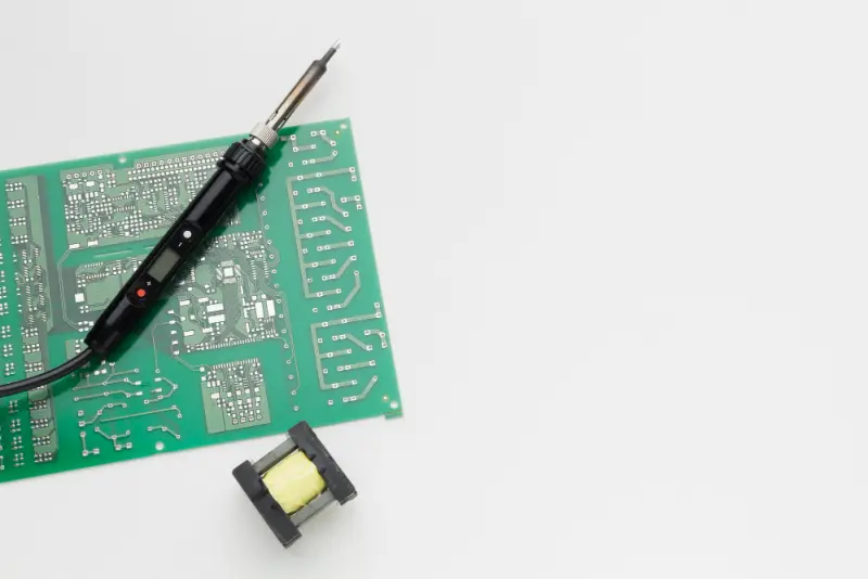
 PCB Assembly
 Layer Buildup
 SMD-Stencils
 PCB Design-Aid & Layout
 Mechanics
 Surface
 Quality
 Drills & Throughplating
 Factory & Certificate


Introduction
In the structured New Product Introduction (NPI) process, PCB prototyping has evolved beyond its traditional role as a concept validation tool to become a crucial strategic phase in the product development cycle. In today's fast-paced electronics market, prototype boards are more than just a physical representation of a circuit schematic; they are a critical step used to verify design, expose signal integrity, thermal, or EMI risks, and establish a solid foundation for large-scale manufacturing.
This guide aims to provide a comprehensive overview for PCB engineers, focusing on the key stages from concept to actual fabrication. It will systematically explore core principles of Design for Manufacturability (DFM), stackup and material selection, impedance control, High-Density Interconnect (HDI) technology, preparing a standard data package, and managing costs and quality assurance. By delving into these essential topics, this guide is designed to help engineers strategically plan their prototyping projects, maximize success, and effectively mitigate risks and costs when transitioning from R&D to mass production.

Table of Content
- Chapter 1: Strategic Differences Between PCB Prototyping and Mass Production
- Chapter 2: Core Principles of Design for Manufacturability (DFM)
- Chapter 3: The Data Package - The Bridge from Design to Manufacturing
- Chapter 4: Cost, Lead Time, and Quick-Turn Capabilities
- Chapter 5: Prototype Quality Control and Testing Methods
- Conclusion and Outlook
Chapter 1: Strategic Differences Between PCB Prototyping and Mass Production
1.1 The Role of Prototyping in the New Product Introduction (NPI) Process
New Product Introduction (NPI) is a structured process that transforms a product idea into a complete, reproducible end-product. It typically covers multiple phases, from ideation, definition, and design to testing, pre-production, and volume manufacturing. PCB prototyping plays an indispensable role in the NPI process, particularly in the "design" and "testing" phases. It transforms a theoretical design into a physical circuit board to validate functionality, test overall performance, and evaluate the design's strengths and weaknesses. By identifying and correcting issues in the early stages, engineers can significantly reduce the complexity, time, and costs that may arise later in the pre-production or mass production phases. A robust prototyping strategy is a powerful tool for accelerating time-to-market, optimizing costs, and improving quality and yield.
1.2 Comparative Analysis of Prototyping vs. Mass Production
PCB prototyping and mass production are two fundamentally different processes, with significant variations in purpose, cost structure, and methodology. Understanding these differences is crucial for choosing the correct path for a project.
- Lead Time and Quantity: Prototyping prioritizes speed to enable rapid design iteration and innovation validation. Manufacturers can deliver rapid PCB prototypes in as little as 24-48 hours. Typical orders are small, ranging from 5-10 boards, which is sufficient for concept validation. In contrast, mass production prioritizes efficiency and scale, with lead times of 4-6 weeks and order volumes of hundreds or thousands of boards.
- Design Flexibility and Iteration: The design in the prototyping phase is highly flexible, and manufacturers often accommodate frequent design changes to help engineers test and resolve issues. In mass production, any design changes are costly and risky. Modifying a layout may require redoing photomasks, scrapping components, and adjusting processes, leading to delays and price increases.
- Quality Priorities and Testing: The primary goal of a prototype board is functional validation, so its testing is relatively less rigorous. The focus of testing is to ensure that basic functions work properly, rather than meeting strict long-term reliability standards. Quality control in the mass production phase is much more rigorous. Factories implement extensive testing, including solderability checks, circuit integrity audits, and environmental stress screening (e.g., IPC-A-600 standards) to ensure high yields and long-term reliability to prevent product failures in the field.
- Cost Structure: Due to the lower efficiency of small-batch production, the per-unit cost of a prototype board is typically higher. However, the total expenditure for early validation is usually modest. Mass production minimizes per-unit costs through economies of scale. Factories require significant investment in automated equipment and custom testing fixtures, so they need large-volume orders to amortize these costs.
- Materials and Manufacturing Tools: Prototyping tends to use simplified, rapid materials and techniques, such as rolled copper and FR-4 substrates. The manufacturing tools are also more modular and flexible, for example, using Laser Direct Imaging (LDI) equipment for quick design revisions. Mass production uses advanced, high-precision technologies and materials, such as high-purity oxygen-free copper and advanced substrates like Rogers, and relies on fixed, high-precision automated tools like multi-head pick-and-place machines and automated inspection systems.
1.3 Why Designing for Prototypes is Crucial?
The true value of prototyping is not in its own perfect functionality, but in its strategic role as a "defect finder" and "risk quantifier." Many engineers see a prototype as a "working" version of a product and expect it to work flawlessly. However, the true value of a prototype lies in its ability to expose design flaws in the physical world that may be unpredictable in digital simulations, such as thermal issues, signal integrity problems, or component compatibility issues.
Solving problems in the prototyping phase can save a significant amount of money compared to fixing them later in production. It is estimated that the average cost of each design re-spin is more than $25,000. Therefore, identifying and correcting problems at an early stage, for example, by conducting a DFM audit, can significantly reduce or even eliminate the need for future rework. This strategic shift from "fixing" to "preventing" moves costs from a high-risk later stage of the project to a more controllable early stage. Although the per-unit cost of a prototype board is higher, the cost savings and risk mitigation it brings to the entire product lifecycle are substantial.
Understanding prototyping's strategic value is step one for risk reduction. Get a free preliminary DFM analysis from NextPCB to detect manufacturability issues in 24 hrs:
Chapter 2: Core Principles of Design for Manufacturability (DFM)
DFM (Design for Manufacturability) is the practice of tailoring your PCB layout to suit the capabilities and constraints of fabrication and assembly processes. Implementing DFM at the prototyping stage is crucial because it helps identify issues early, ensures design stability, and paves the way for a smooth transition to mass production.
2.1 Component Placement and Footprints
- Safety Clearance: Component crowding is a primary cause of automated pick-and-place machine errors and defects (such as "tombstoning"). To avoid such problems, it is recommended to maintain a minimum clearance, such as no less than 0.2 mm for small Surface-Mount Devices (SMDs) and 0.5 mm for larger Integrated Circuits (ICs) like Quad Flat Packages (QFPs). > How to Create a Centroid(Pick and Place) File Instantly?
- Uniform Orientation for Polarized Components: Aligning all polarized components (such as diodes and electrolytic capacitors) in the same direction can reduce programming time for automated equipment by up to 10%, thereby simplifying the production process.
- Component Grouping: Placing similar components (such as resistors and decoupling capacitors) together can reduce the pick-and-place machine's cycle time. For complex boards, this can save 15-20% on assembly time.
2.2 Traces and Spacing
- Trace Width: The relationship between current, trace width, and temperature rise is detailed in the IPC-2152 standard. This standard offers a comprehensive guide that considers parameters such as copper thickness, trace location (internal vs. external), and the surrounding environment. However, it is important to note that the standard's formulas were developed from simple test boards and may overestimate the required copper area for complex, modern designs with multiple heat sources. For this reason, a single, fixed value for a given current load is not absolute; engineers should account for other factors like ambient temperature, parallel traces, and heat dissipation. Traces that are too narrow (e.g., 3 mils) can reach the limits of standard etching processes, increasing the risk of under-etching or open circuits. Most manufacturers recommend a minimum outer layer trace width of 6 mils to ensure reliability.
- Spacing: Trace spacing is equally critical. A 4-mil gap might be theoretically feasible, but considering a ±1 mil etching tolerance, it could lead to a short circuit. For high-voltage designs, IPC-2221B provides guidelines for clearance and creepage distances, which depend on factors such as peak voltage, contamination levels, and board materials. The standard aims to prevent issues like dielectric breakdown and anodic filamentation by specifying minimum conductor spacing. For instance, it provides a table with minimum clearance values for different voltage ranges.
2.3 Via Design and Routing
Vias are conductive paths that electrically connect different layers of a PCB, and their design directly impacts cost, routing density, and signal integrity.
- - Through-hole Vias: Pass through the entire board. They are low-cost but consume routing space.
- - Blind Vias: Connect an outer layer to an inner layer but do not penetrate the entire board.
- - Buried Vias: Connect only two or more internal layers.
- - Microvias: Have a diameter of less than 150 micrometers, typically created by laser drilling.
> Recommend reading: Blind Vias and Buried Vias: What Is the Difference in PCB?
- HDI applications: Microvias are a core component of High-Density Interconnect (HDI) designs. They enable higher routing density without adding more layers and simplify BGA breakouts.
- Special Via Technologies:
- - Via-in-Pad Plated Over (VIPPO): Involves placing a via directly within a pad. This structure can eliminate the trace between the BGA pads and the vias, thereby reducing parasitic inductance and capacitance, and improving signal integrity.
- - Back drilling: For high-speed signals, the unused portion of a via can form a "stub," leading to signal reflections and performance degradation. Backdrilling removes these stubs to achieve a cleaner signal. For designs with increased complexity, like those with board thicknesses greater than 120 mils and signal speeds reaching 25 GHz or more, backdrilling VIPPO structures becomes essential.
The table below provides a comparison of different via types to help engineers weigh the trade-offs between cost and performance.
|
Via Type |
Physical Structure |
Advantages |
Disadvantages |
Typical Application |
|
Through-hole |
Passes through the entire board |
Lowest cost, simple to manufacture |
Consumes valuable routing space, low density |
General-purpose, low-cost designs |
|
Blind |
Connects an outer layer to an inner layer, does not penetrate the entire board |
Saves inner layer space, improves routing density |
More complex to manufacture, increases cost |
HDI, high-density routing |
|
Buried |
Connects only internal layers |
Saves outer layer space, improves signal integrity |
Most complex to manufacture, highest cost |
High-end HDI, high-density, multi-layer boards |
|
Microvia |
Laser-drilled, diameter less than 150μm |
Extremely high routing density, simplifies BGA breakout |
Complex to manufacture, high cost |
HDI, miniaturization, high-processing-power designs |
2.4 Stackup Design and Material Selection
- Stackup Design: A stackup refers to the arrangement of copper and insulating layers on a board. An optimized stackup design can minimize EMI, reduce impedance and crosstalk, and improve electromagnetic compatibility.
- - 4-layer board: A standard 4-layer PCB stackup usually consists of Top Signal Layer, a Ground Plane, a Power Plane, and a Bottom Signal Layer. This arrangement provides a balance between cost and performance for many applications.
- - 6-layer board: A common 6-layer PCB stackup might include a Top Signal Layer, a Ground Plane, a Signal Layer, a Power Plane, a Signal Layer, and a Bottom Ground Plane. This offers more flexibility in routing and improved signal integrity compared to 4-layer designs. > Recommend reading: Best 6-Layer PCB Stackups for Signal Integrity & Impedance Control
- - 8-layer board: An 8-layer PCB stackup might be arranged as Top Signal Layer, Ground Plane, Signal Layer, Power Plane, Ground Plane, Signal Layer, Ground Plane, and a Bottom Signal Layer. This configuration offers maximum flexibility and performance for complex designs.
- Materials Selection:
- - FR-4: Fiberglass and epoxy resin composite material, which is strong, lightweight, and resistant to heat and moisture. It is the most common and cost-effective material, used in over 90% of all PCB projects.
- - Low-Loss Materials (e.g., Rogers): Designed specifically for high-frequency applications (e.g., RF/microwave). FR-4's limitations, such as high dielectric loss, lower thermal conductivity, and limited temperature range, make advanced materials necessary for high-frequency or high-power designs.
The table below provides a detailed comparison of the electrical and thermal properties of FR-4 and Rogers materials.
|
Property |
FR-4 |
Rogers |
Performance Impact |
|
Dielectric Constant (Dk) |
3.4 to 4.8 |
Less than 3 to 10 |
Affects impedance control; Rogers materials are more consistent over a wide frequency band. |
|
Dielectric Loss (Df) |
0.012 to 0.02 |
Less than 0.01 |
Affects high-frequency signal attenuation; Rogers materials' low dielectric loss makes them suitable for RF/microwave applications. |
|
Glass Transition Temp (Tg) |
130 to 180°C |
~280°C |
Determines material stability at high temperatures; Rogers materials have higher temperature resistance, suitable for lead-free soldering. |
|
Coefficient of Thermal Expansion (CTE) |
XY: 16 ppm/°C, Z: 70 ppm/°C |
XY: 15 ppm/°C, Z: 25 ppm/°C |
Affects PCB dimensional stability; Rogers materials' low CTE helps maintain dimensions and reduces stress on solder joints. |
Unclear how material choice impacts signals?
Use NextPCB's Impedance Calculator to simulate performance with your stackup (Supports hybrid materials & HDI microvias):
2.5 Controlled Impedance and Signal Integrity
- Controlled Impedance: For high-speed signal transmission, controlled impedance is crucial, as it prevents signal reflections and distortion. It is achieved by controlling trace width, spacing, copper thickness, dielectric thickness, and the Dk value.
- Microstrip and Stripline:
- - Microstrip: A signal trace located on the outer layer of the PCB, surrounded by the PCB material and air. Its propagation mode is Quasi-TEM, which makes its characteristic impedance frequency-dependent.
- - Stripline: A signal conductor located on an inner layer, sandwiched between two ground planes. Its electromagnetic field is fully contained within the dielectric, making the propagation mode purely TEM, so the characteristic impedance does not vary with frequency.
The table below provides a detailed comparison of the key characteristics of both transmission lines.
|
Property |
Microstrip |
Stripline |
|
Placement |
Outer layer |
Inner layer |
|
Propagation Mode |
Quasi-TEM, characteristic impedance varies with frequency |
Pure TEM, characteristic impedance does not vary with frequency |
|
EMI Shielding |
Open structure, signal easily radiates outward |
Enclosed structure, provides excellent EMI shielding |
|
Routing Density |
Suitable for high-density routing |
Lower routing density, limited by heat dissipation |
|
Propagation Speed |
Relatively faster |
Relatively slower |
- Impedance Testing: The final verification of impedance control is performed using a Time Domain Reflectometer (TDR) on a test coupon. A test coupon is a specialized test structure added by the manufacturer to the PCB panel. The TDR measures impedance by analyzing the changes in the amplitude of the reflected waveform after feeding a pulse onto the transmission line on a test coupon. Typical manufacturing tolerances are ±10% for standard orders and can be as low as ±5% for advanced technology orders. If the measurement on a test coupon is out of tolerance, the entire production panel will be rejected.
2.6 Design for Assembly (DFA) and Panelization
- Silkscreen & Solder Mask: For high-speed signals, it is critical to keep the solder mask away from traces as it can alter the dielectric properties, causing impedance discontinuities. Solder mask, particularly on outer layers, can affect the impedance of a trace, typically reducing it by a few ohms depending on its thickness and dielectric constant. For high-frequency designs, it is critical to account for this effect during modeling. The silkscreen, typically printed on top of the solder mask, has a minimal electrical impact. For silkscreen legibility, a minimum font size of 0.035 inches (0.89 mm) and a line width of 0.006 inches (0.15 mm) is recommended. Silkscreen should not be placed over pads, vias, or high-speed signal lines.
> Recommend reading: DFA in DFMA: Avoid Costly PCB Assembly Errors | NextPCB Case Studies
- Panelization: Panelization is the process of combining multiple individual PCB designs onto one large panel for manufacturing, to maximize material utilization and improve production efficiency.
- - V-Cut (V-Scoring): This involves scoring a V-shaped groove along the edges of the board. It is suitable for boards with regular shapes and straight separation lines, resulting in cleaner edges.
- - Mouse Bites: This involves drilling a series of small holes along the separation line to create a weak point. This method is cost-effective and flexible, making it the preferred choice for prototypes, small batches, or boards with irregular shapes.
Chapter 3: The Data Package - The Bridge from Design to Manufacturing
Submitting correct and complete design data is key to efficient production. The evolution of file formats reflects the industry's demand for higher automation and fewer errors.
3.1 Core File Formats Overview
- Gerber Files: The most widely used format, which essentially is a 2D image for each layer (e.g., copper traces, solder mask). Its limitation is the lack of design rules, net connectivity, or component library information, requiring multiple files for a complete package.
- ODB++: A newer, all-in-one format that consolidates almost all production and assembly information into a single file. It reduces the risk of missing files and errors between design and production. ODB++ is a proprietary standard, but it has become a virtual standard due to its wide support.
- IPC-2581: A modern, open, and unified XML-based standard that integrates all data required for manufacturing, assembly, and testing into a single file. This approach preserves design intelligence and facilitates a seamless, bidirectional data exchange between designers and manufacturers.
The table below provides a comparison of the three main file formats.
|
Format |
Characteristics |
Contents |
Advantages |
|
Gerber |
2D image, layered representation |
Image data per layer |
Industry standard, highly versatile |
|
ODB++ |
All-in-one data package, proprietary |
All production and assembly information |
Reduces file loss, lowers production error risk |
|
IPC-2581 |
Open, unified XML standard |
All design, manufacturing, assembly, and testing data |
High data integrity, reduces manual work, supports automation |
3.2 Complete PCB Prototype Data Package Checklist
Regardless of the format chosen, a complete file package should include the following key information.
- Fabrication Data Package:
- - Gerber/ODB++/IPC-2581 files: Contains design data for all copper, solder mask, silkscreen, board outline, and drill layers.
- - Drill files: Lists drill sizes, quantities, and locations, distinguishing between plated (PTH) and non-plated (NPTH) holes.
- - Fabrication drawing: Includes board dimensions, layer stackup, materials, surface finish, impedance details, and drill chart.
Assembly Data Package:
- - BOM (Bill of Materials): A detailed list of all components, manufacturer part numbers (MPN), supplier part numbers (SPN), and quantities.
- - Pick-and-Place file (or Centroid file): Contains each component's center coordinates (X-Y), rotation angle, and side of the board for automated placement.
- Testing and Quality Assurance Files:
- - Netlist: Defines the connectivity of all nets on the circuit board, used for bare board electrical testing (E-Test).
Try NextPCB Free Online Gerber Viewer
Chapter 4: Cost, Lead Time, and Quick-Turn Capabilities
4.1 Key Factors Influencing Prototype Costs
Prototype costs are primarily determined by the following factors.
- Board Layer Count and Size: A larger board size and higher layer count require more materials and more complex manufacturing processes, which drives up the cost.
- Materials and Surface Finishes: Inexpensive FR-4 is the preferred prototyping material. Advanced materials like Rogers or polyimide can double the cost. Surface finishes like ENIG (Electroless Nickel Immersion Gold) are also more expensive than HASL (Hot Air Solder Leveling).
- Order Quantity: Due to economies of scale, the larger the batch, the lower the per-unit cost.
- Design Complexity: Advanced features such as impedance control, blind/buried vias, VIPPO, and backdrilling will significantly increase the cost.
> Reference for a comprehensive cost analysis of custom pcb & pcba
4.2 Understanding Quick-Turn Services
- Definition and Advantages: A quick-turn service (also known as quick PCB) is the process of manufacturing PCBs in a significantly shorter time frame than the standard lead time (2-4 weeks), typically in 24 hours to 10 days. Its advantages include accelerating time-to-market, reducing development risks, and meeting urgent needs.
- Impact on Lead Times:
- - Design Complexity: High layer counts, blind/buried vias, and HDI features can extend the lead time.
- - Material Availability: Standard materials (e.g., FR-4) are typically in stock, while specialty materials (e.g., Rogers) may require extra sourcing time.
- - Data Package Integrity: Missing files or inconsistent information (e.g., Gerbers not matching the fabrication drawing) can put an order on hold, extending the lead time.
4.3 Balancing Cost and Time
The term "quick" in prototyping is not always the optimal solution. Engineers must strategically balance speed, cost, and technical feasibility. Although quick-turn services save time, their per-unit cost is higher. Additionally, to achieve speed, quick-turn factories may compromise on certain technical capabilities, such as complex stackups or tight impedance tolerances.
For a simple functional verification, a prototype using the cheapest materials and the fastest lead time may be sufficient. However, for a complex design requiring high-speed signal testing, a manufacturer capable of providing controlled impedance and backdrilling must be chosen, even if the lead time and cost are higher. This is a strategic shift in mindset from "fast" to "appropriate."
Get real-time quotes optimized for speed:
Chapter 5: Prototype Quality Control and Testing Methods
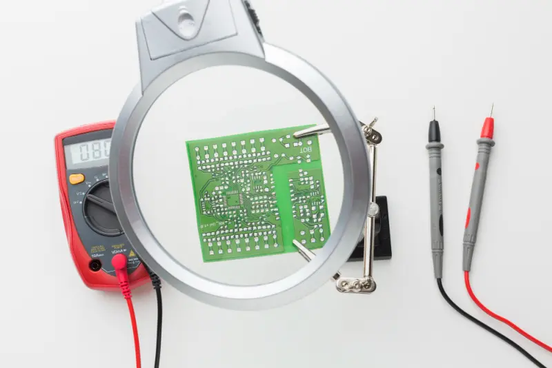
5.1 Quality Assurance in the Manufacturing Phase
- Bare Board Electrical Test (E-Test): E-Test checks the electrical continuity of an unpopulated bare board. It verifies for short circuits and open circuits based on the netlist file.
- - Flying Probe Test: A fixtureless method that is cost-effective for small-volume production.
- - Fixture Method (Bed of Nails): This method requires a test fixture but, once created, allows for rapid testing, making it suitable for mass production systems.
-
Automated Optical Inspection (AOI): This method automatically inspects the image of a bare or assembled board and compares it with design data to find defects that an E-Test might miss, such as conductor traces that are narrowed but still unbroken.
-
X-Ray Inspection: This is primarily used to check for layer misalignment during the lamination of multi-layer boards. For packages like BGAs, X-ray inspection is the only method to check the quality of solder joints.
5.2 Quality Assurance in the Assembly Phase
- Prototype Assembly Process:
- - Solder Paste Printing: Solder paste is precisely applied to the pads on the PCB surface. > Circuit Board Solder
- - Component Placement: Components are placed using automated pick-and-place machines for Surface Mount Technology (SMT) or by hand for Through-Hole Technology (THT).
- - Reflow Soldering: Boards pass through a reflow oven to permanently solder SMT components to the pads under a carefully optimized thermal profile.
- Functional Testing and Debugging: After assembly, the prototype undergoes rigorous functional testing to verify its performance meets design specifications. This includes signal testing, voltage/current measurement, and component validation.
5.3 Test Coupons and Quality Traceability
Test coupons are more than just tools for measuring impedance; they are crucial documents for manufacturing process quality control and traceability. The final verification of impedance control is performed using a TDR on a test coupon. If the measurement on a test coupon is out of tolerance, the entire panel will be rejected. This demonstrates that manufacturers must perform quality validation in every production batch, as each production run is a one-time process. By requesting that the manufacturer provides the test coupons, engineers can independently verify the manufacturer's quality commitment and use them as a basis for future audits and quality traceability.
Conclusion and Outlook
PCB prototyping is an indispensable strategic step in new product development. It is far more than simply transforming a design into a physical entity; it is about actively identifying and mitigating risks to lay a solid foundation for successful mass production.
The core takeaways of this guide can be summarized as follows:
- Prototyping vs. Production: They are two complementary stages in the NPI process, each with a different focus. Prototyping prioritizes speed and iteration, while production prioritizes cost and yield.
- DFM: It is a guiding principle that runs throughout the entire process. Early investment in DFM can avoid the high costs of rework later.
- Data Package: A complete and accurate data package is the foundation for effective communication with the manufacturer. The evolution from Gerber to IPC-2581 demonstrates the industry's demand for automation and data integrity.
- Cost and Lead Time: Quick-turn services offer time advantages, but engineers must strategically balance speed, cost, and technical capabilities.
- Quality: Quality control is integrated into every stage of manufacturing and assembly, and tools like test coupons and E-Test are necessary for verifying quality.
This guide is designed to empower engineers to make informed design decisions and build effective collaborations with manufacturing partners. By viewing PCB prototyping as an integrated, multi-disciplinary challenge, engineers can ensure their innovative ideas can robustly and reliably transition from the lab to the market.
> Further reading: Mastering Prototype Assembly for Your PCB Board Prototype
From proof-of-concept to mass production: NextPCB delivers full engineering support:
✦ 24-hr DFM Feedback | ✦ 72-hr Rapid Prototyping | ✦ 600K+ Pre-Verified Parts
Register a Single Account for All HQ NextPCB Services


