
 NextPCB Capabilities
Printed Circuit Boards
NextPCB Capabilities
Printed Circuit Boards
 PCB Assembly
 Layer Buildup
 SMD-Stencils
 PCB Design-Aid & Layout
 Mechanics
 Quality
 Drills & Throughplating
 Factory & Certificate
 PCB Assembly Factory Show
Certificate
PCB Assembly Factory Show
Certificate
Support Team
Feedback:
support@nextpcb.com


Are you interested in learning about PCB cloning and the benefits it can offer? With the help of modern technology and its advancement, Printed Circuit Board (PCB) cloning has become an efficient and cost-effective way of manufacturing.
PCB cloning involves replicating the same design and features of an existing board to provide a cost-effective alternative. In this article, you'll find out everything you need to know about PCB cloning, including its benefits and legal boundaries.
Read along and learn why PCB cloning is invaluable for many professionals and industries.
In this article,
A PCB clone is a precise replication of the exact details of an existing PCB design. The PCB cloning process involves copying the features and specifications of a particular PCB, the product of which is called a PCB clone, also known as a PCB copy board, PCB board copy, circuit board clone, PCB duplication, or PCB reverse development. Electronics manufacturers use them to produce high-quality electronic components quickly and cost-effectively.
This technology has become increasingly popular in recent years, allowing companies to produce identical copies of PCB circuits and components without designing and manufacturing them from scratch. It is usually done by analyzing and studying the electronic circuit based on the information provided in a manufacturing file, including its circuit board layout, schematic, and components.
To successfully clone the board, PCB reverse engineering is carried out, which involves using software and hardware tools, as well as professional expertise. It provides a great way to save time, money, and resources during product development and is becoming increasingly popular in the PCB industry.
PCB cloning can be a complex process that requires careful planning and precision to get the desired results. It is a reverse engineering technology process that uses existing PCB boards to create a replica. Here are the detailed steps you need to know when cloning a PCB.
Before starting the PCB cloning process, it is essential to have a clear understanding of the design you wish to clone and the requirements to complete the project successfully.
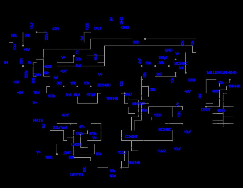
Ensure you have the Bill of Material (BOM) and a copy of the schematic diagram of the existing PCB. The schematic is the blueprint of the circuit design, showing how the components are interconnected. It will help you understand the electrical parameters, such as voltage, current, and power requirements.
The best way to get a schematic diagram for the original board is to contact the manufacturer. Usually, the manufacturer provides a detailed schematic diagram of the board. If the manufacturer does not provide a schematic diagram and the original board is unavailable, purchasing a PCB repair manual containing schematics for different board types may also be possible.
Alternatively, there are available resources online that specialize in providing schematics for various types of boards. Often, it's possible to find a schematic diagram on resource repository sites such as GitHub or other similar resource-sharing sites.
Once the schematic diagram is on-hand, it is important to take the time to review it carefully. Examine the diagram of the board and each component to understand how the interconnection of each component. This can help to ensure that the clone will be as accurate as possible.
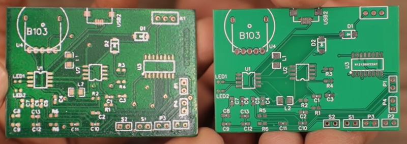
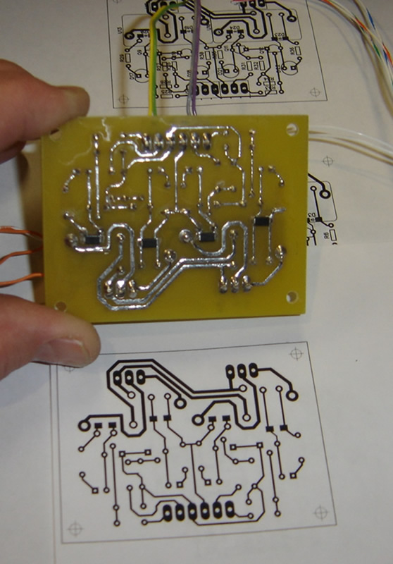
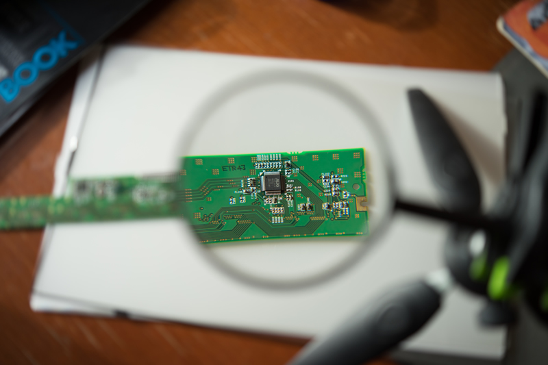
Take photographs of every layer of the board. Using a digital camera, take multiple pictures of every layer of the board from various angles if possible. Keep track of all components on the board, including the type, parameters, and positioning. Pay special attention to the direction of diodes, triodes, inductors, transistors, and integrated circuit chips.
Carefully remove all surface-mounted components and mechanical connectors, such as sockets and terminals. Clean the PCB board surface with alcohol and place it into a scanner. Make sure to raise some scanned pixels slightly to get a clear image.
a) Load the image into a photo editing software such as Photoshop. Scan the board in color to capture all markings, logos, text descriptions, and designators on the printed circuit board. Save the file, then print it out for reference.
b) Slightly polish the top and bottom layers of the board with water-dyed paper, ensuring the copper film is bright.
c) Place the board back into the scanner. Open your photo editing software to scan both layers separately in color. Ensure the board is placed horizontally and vertically in the scanner to maintain accuracy.
d) Adjust the contrast and darkness of the canvas so that portions with the copper film clearly separate from those without copper film. If there are any issues with the images, use the photo editing software to repair them. Turn the images into black and white to check if the lines are clear; if not, repeat this step until they are.
e) Save the images as black and white BMP format files (TOP.BMP and BOT.BMP).
PCB file formats are an essential component of electronic design and manufacturing. Two of the most popular file formats are Gerber and CAD. For this instance, a CAD file will be generated.
f) You'll need to use software for PCB design to convert the two BMP files to PCB file format. Load them into the software, such as Protel or a similar tool, for PCB reverse engineering.
Then, import the CAD file from the PCB editor. Two levels must be generated using the design software.
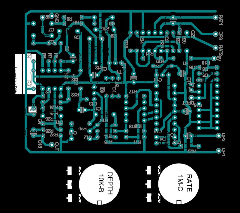
g) Convert TOP.BMP to TOP.PCB, paying special attention to the conversion to the SILK layer. Layout circuitry pattern tracks in the top layer and place components according to the scanned image in (a). Delete the SILK layer.
h) Convert the BOT.BMP of the bottom layer to BOT.PCB and convert it to a SILK layer as well. Trace lines in the BOT layer, then delete the SILK layer.
i) Open the CAD files. Using the PCB image as a reference, copy the component package into the CAD. Arrange the pads according to their sizes. Compare both PAD and VIA layers and ensure the correct placement to determine a discrepancy; if there is, repeat from (b) to (i).
j) Transfer TOP.PCB and BOT.PCB into Protel and combine them into one image diagram.
k) Print the TOP LAYER and BOTTOM LAYER on a transparent film (1:1 ratio) with a laser printer.
Gerber file is a 2-D ASCII format representing each PCB manufacturing layer. It is compatible with most PCB manufacturers and widely considered the industry standard. However, working with multiple files can be challenging, and errors are more common.
CAD files, on the other hand, are more comprehensive and can contain additional valuable data, which enables the communication between the PCB designers and the manufacturer better. The ODB++ and IPC-2581 file formats are examples of CAD, simplifying the process by having all the data in a single file.
Ultimately, the choice between the two depends on the designer's needs and the manufacturer's. It helps to consider this before starting a project. It may also be practical to use PCB design software that provides support for both Gerber and CAD files, giving you the flexibility to choose the best file format for your projects.
Place the printed film on top of the PCB to compare for accuracy. Before beginning the fabrication process with your cloned design, you must ensure the design is accurate and error-free. It's important to take the time to thoroughly review the design and verify the accuracy of the components and connections.
Double-check all the elements and their respective footprints to ensure the schematic is accurate and matches the design's intent. It's also important to check the spacing between components to ensure that everything will fit appropriately. Ensure that all the pins on the components are connected correctly and that all labeling is accurate. Once you have verified the design, you can move on to the layout.
Next, check the board's layout to verify that all the traces are routed correctly and that no components overlap. Ensure that it meets all clearance and spacing requirements and that all the connections line up. Additionally, check the layers of the board to confirm that the trace widths meet the fabrication requirements.
By reviewing and verifying the board design file thoroughly, you can ensure that your PCB clone will be fabricated accurately and meet the desired specifications. This process can be time-consuming, but it's an essential step to ensure your design will be successful.
Once the design files are ready, the next step is to generate the files containing all information about the PCB layout, including layers, components, drill data, outline, and other information needed to fabricate a PCB.
It is critical to inspect every aspect for imperfections or errors carefully. Any discrepancies between the design files should be addressed before the files are submitted for production, as the manufacturer will use this to produce the PCB clone.
This requires a thorough understanding of the design process and adherence to standards and formats. Any additional information should be included to ensure that the manufactured clone will be a close copy of the original PCB as possible.
Upon providing the precise specifications, the design files should be transferred to the PCB fabrication company along with any additional information that may be required. This could include a bill of materials, a component list, or other design notes.
You will then be given an estimated total cost and delivery time. Once you receive the estimate, you must confirm the order before the production process can begin.
When confirming the order, you should double-check the specifications to ensure accuracy and completeness. It's also essential to review the PCB clone service terms and policies to determine any issues or restrictions you should be aware of before confirming the order. Doing so will ensure that you get the PCB clone you requested and that it arrives according to your expectations.
Once the order is confirmed, you will be asked to pay to cover the cost of the PCB clone and any associated fees. After receiving the payment, the manufacturer will begin the production process.
Once you've placed your order and received your PCB clone prototype, testing and inspecting it to ensure it meets the required standards is critical to the cloning process. It allows you to test the functionality of the PCB without the need for costly production runs. Use the prototype PCB to test the design, identify errors or issues, and make necessary modifications to ensure the desired results.
First, visually inspect the PCB clone prototype to ensure it meets your requirements. Specifically, check the size, shape, color, and components. You should also check for defects or flaws and whether the components are properly placed and soldered.
Next, conduct electrical tests such as continuity, power, signal integrity, and thermography tests. These tests help detect any electrical problems with the PCB clone prototype. Using PCB software tools for analysis, simulations, and other tests is also important. This helps identify any potential issues before PCB production.
Once you've visually inspected and tested the PCB clone prototype, ensuring it meets the planned requirements is important. This involves comparing the results of the tests with the planned design. If any test fails, the design should be revised to resolve the problem. Proper packaging is also crucial for protecting the PCB and ensuring it reaches its destination in good condition.
After the prototype has been successfully tested and all necessary modifications have been made, it is time to begin the final production run. Double-check the design parameters and specifications before starting the production run to ensure the desired results.
The PCB cloning process involves several steps, including selecting suitable materials, inspecting the PCB for quality, and conducting the required tests. The entire process takes several days, depending on the project's complexity. Once the PCB clone is complete, it will be shipped to you in the safest and most efficient manner possible.
PCB cloning is a powerful tool for those looking to quickly and effectively replicate existing PCBs and reap their numerous benefits. Let us look at some of those.
One of the most significant advantages of PCB cloning is cost savings. It removes the need to create a new PCB design, which can be time-consuming and expensive. Because PCB cloning allows for a single board to be replicated quickly and accurately, businesses can avoid the costs of designing, prototyping, and manufacturing a completely new board.
Another important benefit of PCB cloning is that it helps improve manufacturing process scalability. By using a cloned circuit board, manufacturers can produce their products with more precision and accuracy while maintaining the same level of quality and making it easier to troubleshoot any issues that may arise.
Additionally, by creating a clone of an existing PCB, engineers can analyze its components and study the design in detail, something that would otherwise be impossible if the board was not cloned or the designs are unavailable. This can help improve their design's efficiency and effectiveness and ensure they are easily reproducible.
Using a PCB clone can greatly reduce time to market by significantly shortening the entire product development process. It enables them to repeatedly use the same proven design without wasting time creating a new one.
By producing a copy of a PCB design, companies can quickly make a prototype, test it, make any necessary changes on the spot, ensure that the final design meets their exact specifications, and move on to the next stage of product development. This is especially helpful for companies testing different designs, as it allows them to rapidly test and modify their boards before committing to a final design.
Cloning a PCB is often essential for manufacturing a product. Many PCB companies may need to produce the same PCB across multiple locations to keep up with demand, replicating the same board precisely in multiple places. Using a PCB clone ensures that the boards used in each location are identical.
PCB cloning enables you to customize designs to fit your specific component needs, create a unique product, or modify an existing design. In addition, many services offer a range of features that simplify creating a PCB clone.
For instance, some providers offer customization of board sizes, layers within a board, and even the thickness of each layer. Some are even offering options for customizing the look of the board, such as adding text, images, and logos. This makes it possible to create boards with different levels of complexity and select components specifically suited to your components and application.
Others also provide additional services that simplify PCB cloning, including design support, PCB assembly, and testing services, helping to ensure that your board is created correctly and meets all your project requirements. By taking advantage of these services, you'll be able to create a PCB clone that is exactly how you want it to be.

When it comes to PCB cloning, there are a few key legal considerations to be aware of. Cloning a PCB is subject to the same intellectual property laws and regulations as the original design. Hence, ensuring you comply with all applicable laws and regulations is essential.
Additionally, it is crucial to be aware of any applicable export or import regulations that may apply to the production and distribution of your cloned PCB. Understanding the legal implications of cloning a PCB can help protect you from potential legal action and financial losses.
It's important to note that finding a reputable PCB manufacturer is vital. This ensures that the output of your project is of the highest quality possible.
NextPCB provides high-quality, low-cost, and fast-delivery PCB prototype services that fully meet the requirements of the ISO9001: 2008 quality management system. Prototype service includes Multi-layer PCBs, 3+N+3HDI, and rigid-flexible boards.
With as fast as 24 hours of lead time, you could receive your board within a week or less. Contact NextPCB and explore how we can be your long-term business partner on your next PCB projects.
PCB cloning allows companies to replicate an existing board quickly and efficiently, and help streamline processes, often saving considerable time and money. It is a great way to produce an exact copy of existing PCBs while allowing the freedom to customize or scale the design as needed.
The process can be essential, especially when a device requires repairs and no information is available, when an out-of-date PCB is no longer available from the original manufacturer, or to make a more cost-effective board version.
Cloning a PCB requires careful consideration to ensure the process is successful and that the resulting clone meets all requirements. There are numerous factors to consider, such as cost, quality, turnaround time, and design flexibility.
Additionally, finding a reputable PCB design and manufacturing company with experience is equally important. It can help ensure that the output is of the highest quality and that the original design is accurately copied.
Whether for cost savings, time-saving advantages, or design flexibility, PCB cloning is a great solution for businesses and individuals looking to get the most out of their projects.
Still, need help? Contact Us: support@nextpcb.com
Need a PCB or PCBA quote? Quote now


 Surface

