
 NextPCB Capabilities
Printed Circuit Boards
NextPCB Capabilities
Printed Circuit Boards
 PCB Assembly
 Layer Buildup
 SMD-Stencils
 PCB Design-Aid & Layout
 Mechanics
 Quality
 Drills & Throughplating
 Factory & Certificate
 PCB Assembly Factory Show
Certificate
PCB Assembly Factory Show
Certificate
Support Team
Feedback:
support@nextpcb.com


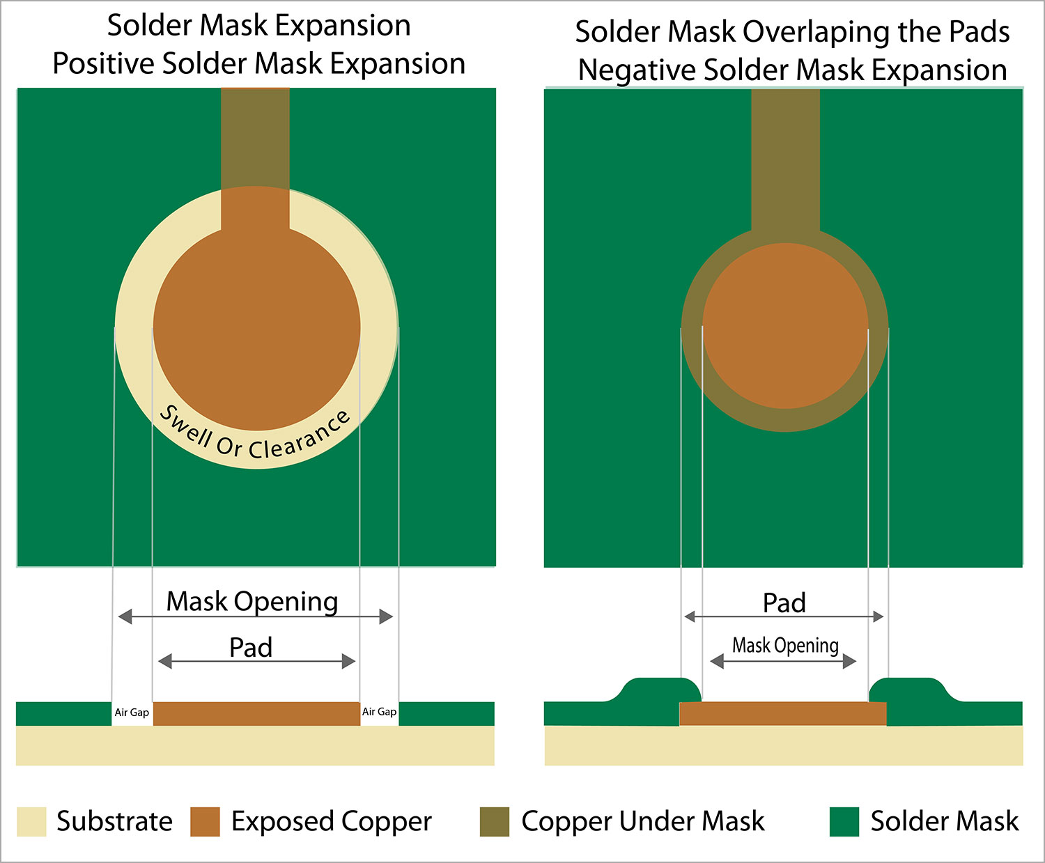
Solder mask expansion, also known as the solder mask swell or solder mask clearance, is a term used in printed circuit board (PCB) design and manufacturing. It refers to the gap or distance between the edge of a copper pad or trace on the PCB and the edge of the solder mask that covers the rest of the board to prevent solder bridging or short circuits during the soldering process.
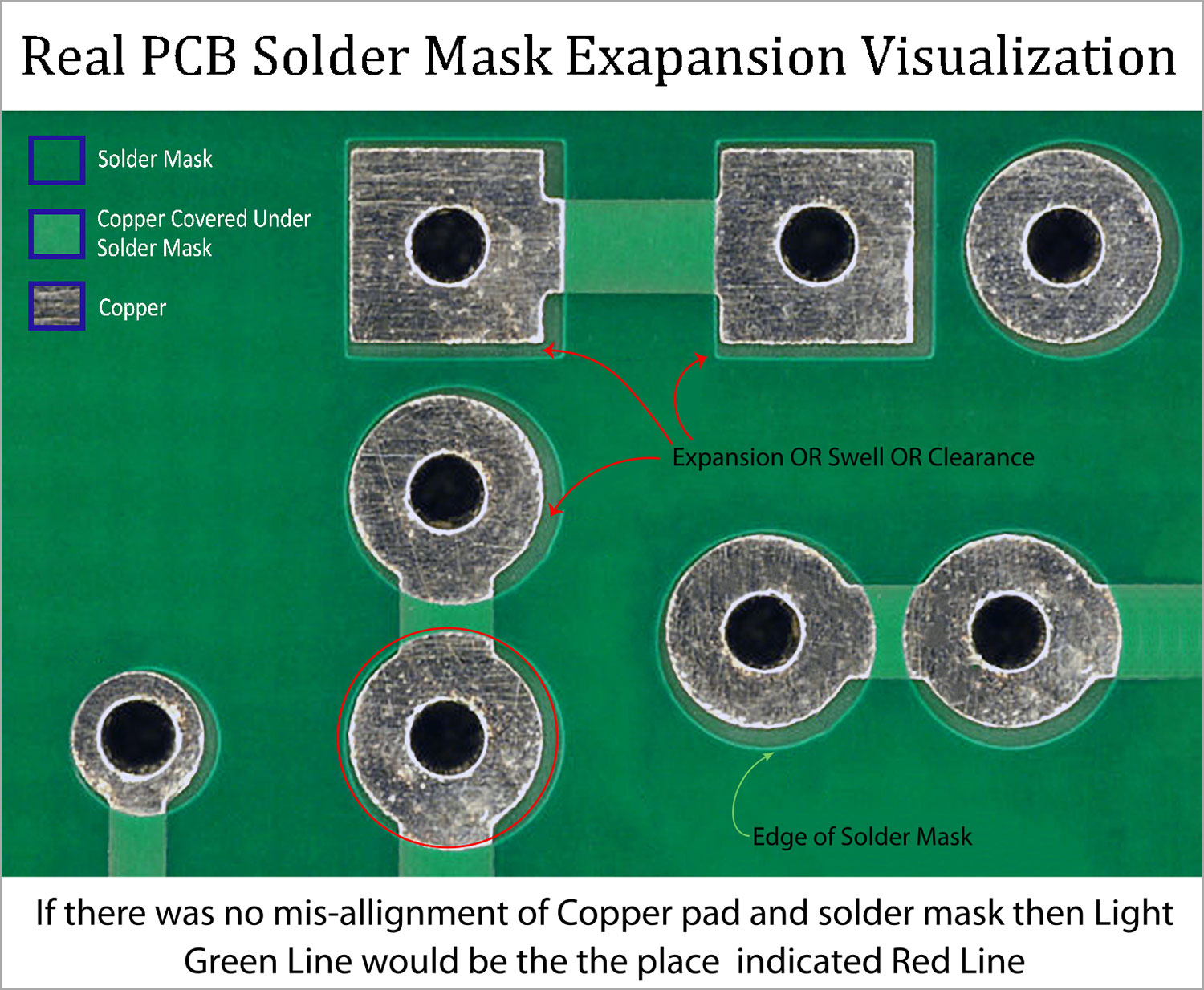
The purpose of the solder mask expansion is to provide sufficient clearance between the solder mask and the copper pad, ensuring that solder only adheres to the exposed pad areas during assembly, while still preventing solder from accidentally spreading to neighboring pads or traces. The expansion size typically depends on the manufacturer's guidelines, but it is generally kept between 2 to 5 mils (0.002 to 0.005 inches) or even larger, depending on the specific application and requirements.
Solder mask expansion is an important consideration in PCB design, as insufficient expansion may lead to solder bridges or shorts, while excessive expansion can make soldering components more challenging and reduce the effective pad area for component attachment.
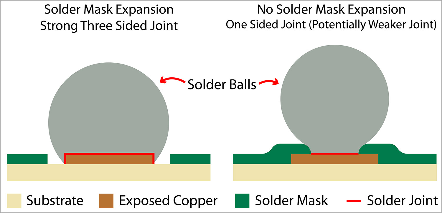
A solder mask is a protective layer applied to a PCB, leaving only the copper pads and traces exposed for soldering components. Solder mask expansion refers to the gap between the edge of a copper pad or trace and the edge of the solder mask. The main purpose of this expansion is threefold: to prevent solder bridging and short circuits, ensure proper solder adhesion to pads, and balance clearance and pad area for effective component attachment.
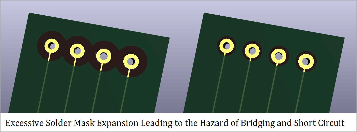
During the soldering process, solder paste is applied to the exposed copper pads to create electrical connections between components and the PCB. If the solder mask expansion is too small, the solder can spread to neighboring pads or traces, creating solder bridges or short circuits, which can lead to malfunctioning devices or even damage.
The solder mask expansion must be large enough to allow solder to adhere only to the exposed pad areas during assembly. This ensures a reliable and robust electrical connection between the components and the PCB. Insufficient solder mask expansion can result in weak connections and ultimately device failure.
Achieving the optimal solder mask expansion is a balancing act. Excessive expansion can make soldering components more challenging, as the pad area available for component attachment is reduced. Designers must find the perfect balance between sufficient clearance to avoid solder bridging and maintaining a sufficient pad area for reliable component attachment.
Several factors can influence the appropriate solder mask expansion value for a specific PCB design. These factors include manufacturer's guidelines, PCB design and layout constraints, and component density and tolerances.
PCB manufacturers typically provide guidelines for the solder mask expansion values they recommend for their fabrication processes. These guidelines take into account the capabilities and tolerances of their manufacturing equipment and processes. It is essential for designers to consult with their manufacturers to ensure that the solder mask expansion values they choose are compatible with the fabrication process.
The complexity of the PCB design and layout can also impact the appropriate solder mask expansion value. For example, a design with a high component density or tight spacing between pads may require smaller solder mask expansions to accommodate the reduced space available. On the other hand, designs with larger, more spaced-out components may allow for more generous solder mask expansions.
The density and tolerances of the components used in the PCB design can also affect the optimal solder mask expansion value. Smaller components with tighter tolerances may necessitate smaller expansions to avoid solder bridging, while larger components with more relaxed tolerances may allow for more considerable expansions.
General industry recommendations for solder mask expansion values range from 2 to 5 mils (0.002 to 0.005 inches). However, the specific value chosen may vary depending on the application and requirements. For instance, designs with high-frequency signals or high-power components may require larger expansions to ensure proper isolation and heat dissipation. Conversely, designs with fine-pitch components may necessitate smaller expansions to accommodate the reduced spacing between pads.
The ideal solder mask expansion value should be determined by considering the specific application and requirements of the PCB design. Factors such as the operating environment, signal integrity, and mechanical stresses can impact the choice of solder mask expansion. For example, PCBs used in harsh environments or subjected to mechanical stresses may require more robust solder connections, thus influencing the solder mask expansion value.
In some cases, specific industry standards or regulations may dictate the solder mask expansion values for certain applications. For instance, in the aerospace and defense industries, more stringent requirements may be imposed to ensure the reliability and robustness of the PCBs used in critical systems. In these cases, designers must adhere to the specified solder mask expansion values to meet the industry standards and regulations.
Improper solder mask expansion can lead to several issues during the assembly and operation of a PCB. These issues can be categorized into two main groups: problems arising from insufficient expansion and problems resulting from excessive expansion.
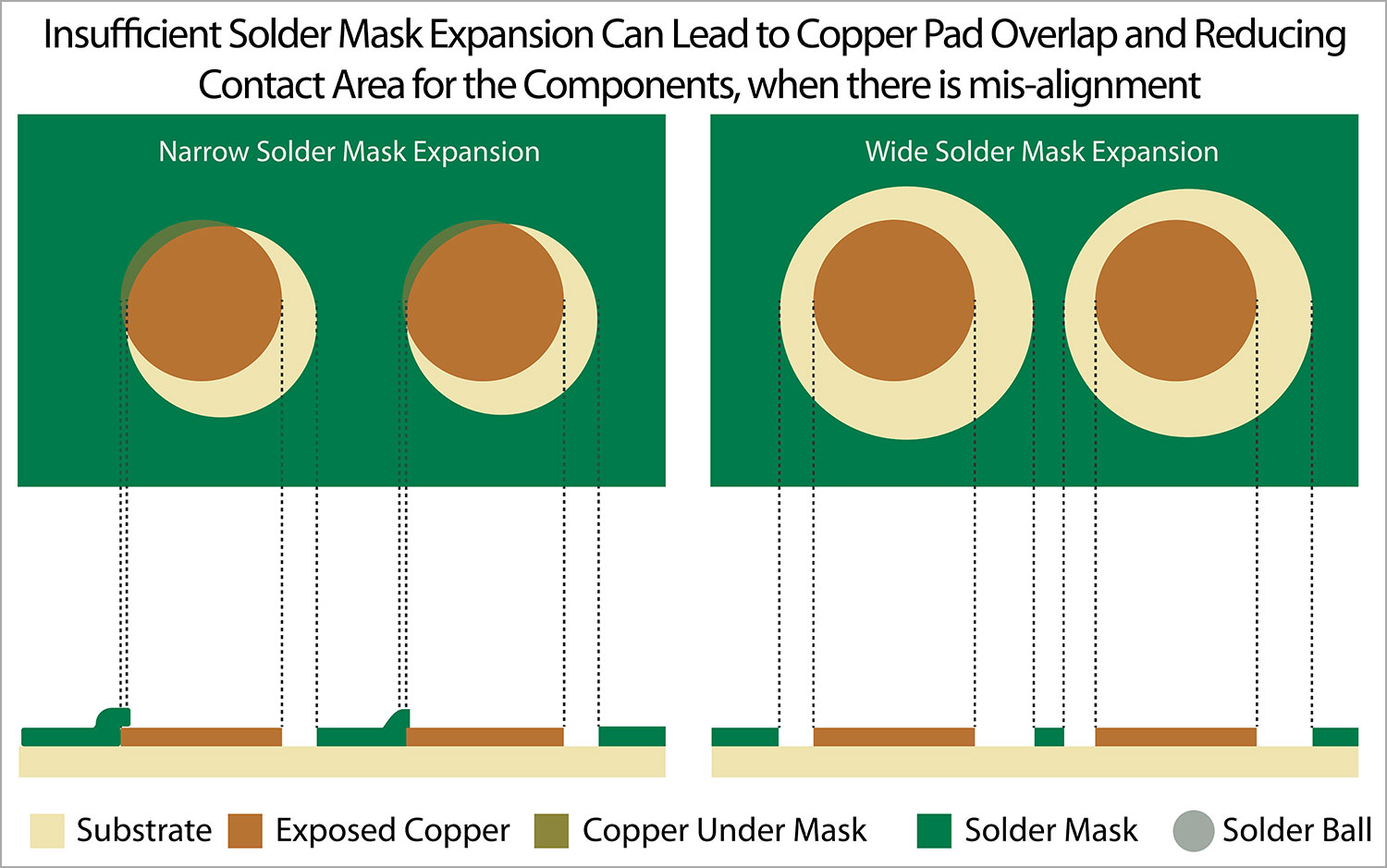
When the solder mask expansion is too small, solder can spread across neighboring pads or traces during the soldering process, creating solder bridges. These bridges can cause short circuits, leading to device malfunctions or even damage.
Short circuits occur when there is an unintended electrical connection between two points in a circuit, allowing current to flow through an unintended path. Insufficient solder mask expansion can result in solder bridging, which creates short circuits that can lead to component damage, PCB damage, or even complete device failure.
When the solder mask expansion is too large, it can make soldering components more difficult. With a reduced pad area, it can be challenging to create reliable and robust solder connections, leading to weak or unreliable electrical connections between the components and the PCB.
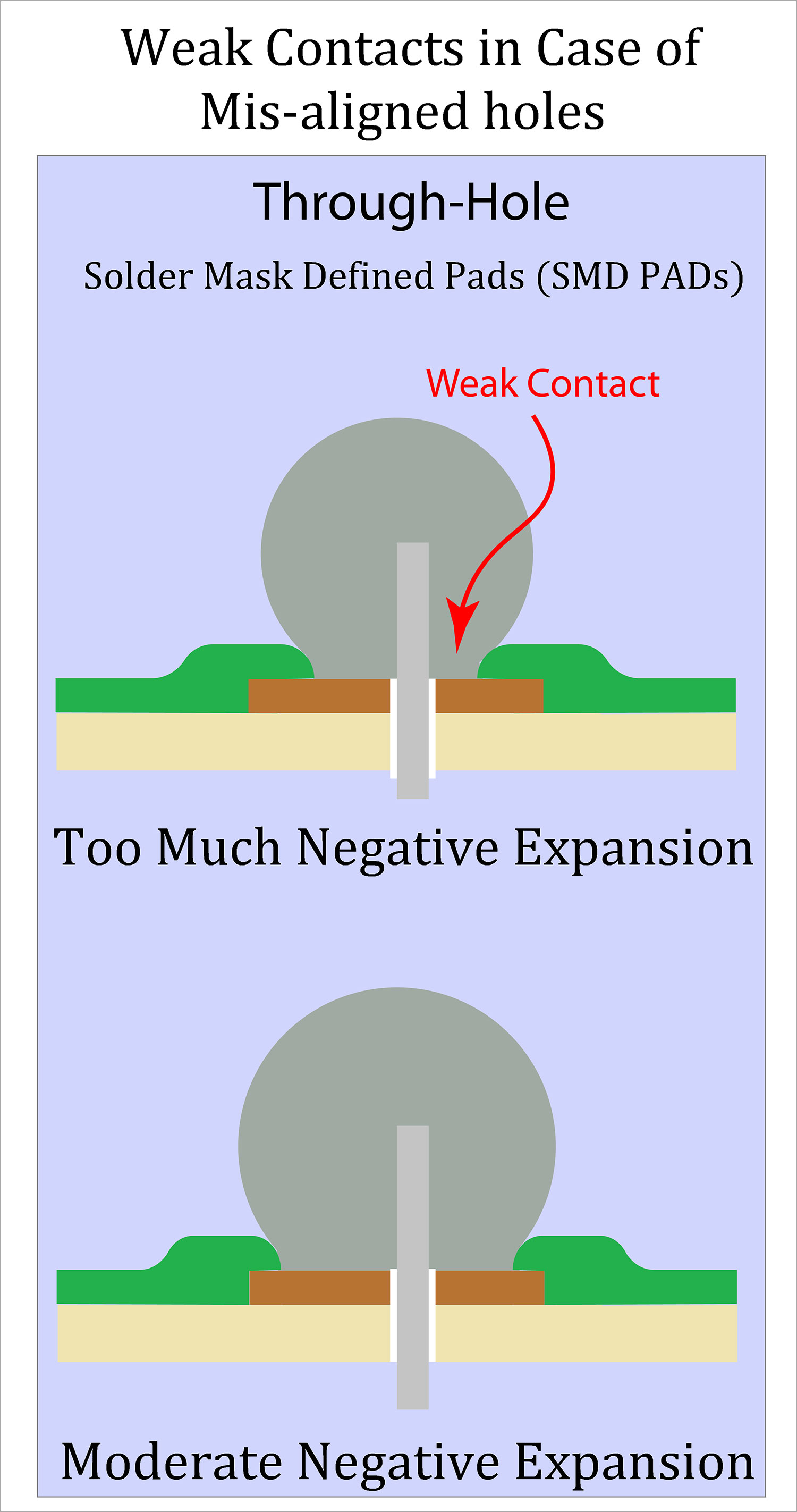
Excessive solder mask expansion can limit the available pad area for component attachment. This can make it difficult to achieve reliable and robust solder connections, potentially leading to device malfunction or failure due to weak or intermittent electrical connections.
Optimizing solder mask expansion is a crucial aspect of PCB design. Designers can employ several techniques and tools to ensure that the chosen expansion values are appropriate for the specific design.
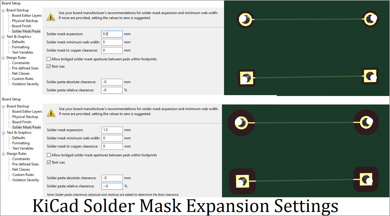
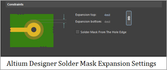
Modern PCB design software often includes features that help designers optimize solder mask expansion. These features may include design rule checks (DRCs) that verify solder mask expansion values against the manufacturer's guidelines or industry standards. Additionally, designers can use the software to visualize the solder mask expansion and make adjustments as needed to accommodate specific design constraints or requirements.
Working closely with PCB manufacturer is essential for ensuring optimal solder mask expansion values. Manufacturers can provide guidelines and feedback on the chosen expansion values based on their experience and the capabilities of their fabrication processes. By collaborating with manufacturers, designers can optimize the solder mask expansion to achieve the best possible results in the final product.
Iterative design and prototyping can also help designers optimize solder mask expansion. By creating and testing multiple prototypes with different solder mask expansion values, designers can identify the optimal value for their specific design. This iterative process can lead to more reliable and efficient PCBs, reducing the likelihood of issues during assembly and operation.
Solder mask expansion is a critical consideration in PCB design and manufacturing, playing a crucial role in the reliability and efficiency of the final product. By understanding the purpose of solder mask expansion, considering factors that influence its optimal value, adhering to typical values and industry standards, and being aware of the consequences of improper expansion, designers can make informed decisions that improve the overall quality of their PCBs.
Collaborating with manufacturers, utilizing advanced PCB design software features, and employing iterative design and prototyping techniques can further aid designers in optimizing solder mask expansion for their specific applications. Ultimately, a thorough understanding and careful consideration of solder mask expansion can result in higher-performing and more reliable electronic devices, ensuring their successful operation in a wide range of applications and environments.
Still, need help? Contact Us: support@nextpcb.com
Need a PCB or PCBA quote? Quote now


 Surface

