
 PCB Assembly
 Layer Buildup
 Online Tools
 PCB Design-Aid & Layout
 Mechanics
 SMD-Stencils
 Quality
 Drills & Throughplating
 Factory & Certificate
 PCB Assembly Factory Show
Certificate
PCB Assembly Factory Show
Certificate
Support Team
Feedback:
support@nextpcb.com


The blackhole metallization process was first patented in 1986 by Hunt, an American company. The hole wall is treated with a dispersed toner suspension and then electroplated. This is the first time that carbon has been applied to the metallization of pores. The process is called "BlackHole." The technology was then resold to MacDermide, where it remains today. MacDermide is in recent years only rapid development, mainly used for the flexible board (FPC) and BT PCB, for rigid PCB cases are not rare. According to the current owners and peer products in the market application situation, NextPCB makes a preliminary analysis and discussion, for the circuit board industry practitioners' reference and correction.
Flexible PCB or Flex Circuits is the type of PCB or circuit board that has bending ability according to our required and wanted shapes. FPC is mainly made of CU (Copper foil) (E.D. Or R.A. copper foil), A (Adhesive) (acrylic and epoxy resin thermoset adhesives), and PI (Kapton, Polyimide) (polyimine films). FPCB has many advantages, such as space-saving, weight reduction, and high flexibility, and is widely used in production and life.
BT PCB (LED cooling substrate, LED aluminum substrate, etc.) mainly refers to a thickness, not more than 1mm, and has bis maleimide triazine as the substrate of the rigid board. These two kinds of substrate have a common point: flexible circuit boards are generally within 0.1 mm. But BT rigid boards are within 1mm, with most through holes and no blind holes and buried holes.
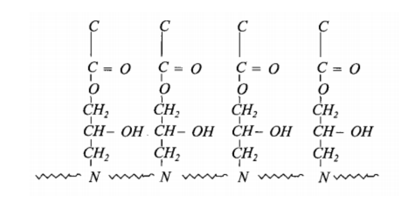
The principle of the blackhole is to adjust the positive charge of the hole wall through the coulomb force to attract particles in a negatively charged dispersed suspension. After drying, a graphite-covered conductive layer is formed on the pore wall. Then you can directly plate the copper in the acid dielectric. The interaction between the pore wall and particle is essentially a chemical reaction of organic functional groups. The regulator can contain heterocyclic compounds containing nitrogen, and the carbon upper band when the graphite particles contact the pore wall, under appropriate conditions, the carbon ring of regulator a opens and the dehydration cross-linking reaction occurs with b. The graphite particles are then chemically bonded to the pore wall. The structure diagram after the cross-linking reaction is as follows:
The technological process of the blackhole method:
Copper clad laminate → cleaning → black holeization → drying → striping → electro-coppering
The concrete practice is:
1. Clean: the purpose is to greasy dirt and other impurities of removing in the printed board through the hole, in helping and the electric of the resin surface, is beneficial to blackhole liquid and adsorbs fully on the hole wall; This operation is carried out in two steps;
2. Black holeization: the printed board is immersed in the liquid of the blackhole, and the temperature remains at 15~40 °C, flood for 1~10 minute, make black hole liquid equitably coated on the hole wall, and contact well in the dielectric base layer, make and deceive the hole plate;
3. Dry: will deceive orifice plate and place vacuum or heat drying under the room temperature, the heating-up temperature is incubated for 20~30 minutes 75~120 ℃ of scopes, can use a far infrared drying machine or other drying plants to carry out, and makes through this operation to form a uniform black thin film in the hole;
4. Striping: through the printed board of the above-mentioned operation, all exposed portions all scribble one deck of black thin film, and this operation is the black thin film of the copper laminar surface will be removed; Carry out in order to follow method:
5. Electro-coppering: will deceiving the hole plate, to immerse concentration be to flood in 5% the sulfuric acid solution, after the taking-up, carries out electric plating of whole board in the acid electroplating bath of routine, and Current Control is at 1~1.5A/dm during plating 2, the time kept 0.5 hours, and thickness of coating reaches 6 μ m and gets the final product.
According to the current process practice, the manufacturing of rigid PCB on the market mostly adopts the traditional PTH (including horizontal and vertical two kinds), especially the manufacturing of HDI PCB. According to the customer's feedback, we summarize the reasons as follows (welcome to leave your comment in the bottom of the article):
According to the customer situation of the blackhole process, the actual distribution of customers using blackholes for rigid PCB is as follows:
Because the thickness of the BT board generally does not exceed 1 mm, the aperture is not less than 0.2 mm. The blackhole process of this kind of product adaptability is good, the number of manufacturers using the blackhole process in the current market segment is more and more in the south and central China market.
The reliability and technology are actually better than the traditional PTH and polymer (conductive film), on account of the smaller thickness ratio (aspect ratio) of a simple rigid PCB in the current process practice. However, market acceptance is not high, but the acceptance is increasing. The blackhole process is still in the stage of promotion and persuasion.
The following table is a comparison of the results of the solder float (288℃) of our company's blackhole process for simple rigid boards. The circuit board tested substrate is FR-4.
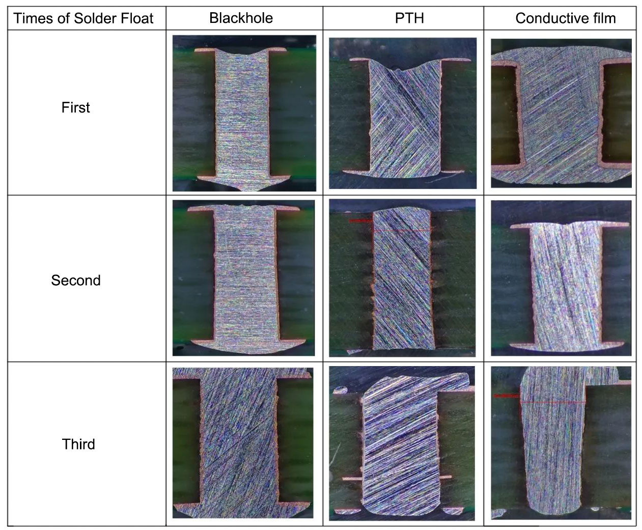
Comparison of test results: For the first solder float, all three are normal; For the second solder float, there was an anomaly of partial copper layer disconnection in PTH. After the third solder float, only the blackhole remained normal, and the hole walls of PTH and polymer (conductive film) were destroyed.
It can be concluded from the comparative test that the bonding force between the copper layer and the hole wall after the blackhole process is better than that of the traditional PTH.
We believe that the reason for this result is that compared with PTH, primary copper is not needed in the blackhole, and the graphite in the toner forms a solid cross-linked structure with the substrate. So there is no common boundary between the copper layer and the electroplated copper layer, resulting in the binding force between the copper layer and the substrate after the blackhole treatment being better than that of the PTH.
At present, the process practice of the blackhole process for HDI boards is only carried out in the laboratory, and there are few cases in the market. The mainstream scheme is still based on horizontal PTH, but the Eclipse and Shadow process, which are similar to the black-hole process, have been successfully applied to HDI.
In summary of the company's customer cases, the advantages and disadvantages of the blackhole process compared with the PTH and conductive film process are mainly reflected in four aspects: high quality, more environmental protection, convenience, low cost, and wide adaptability.
High quality: PTH and conductive film process is a complex chemical reaction, subject to various reaction conditions prone to product quality instability, and poor product consistency (need complex analysis, and control). The blackhole process is a physical adsorption reaction, with high-quality stability, and good product consistency, effectively reducing the hole-breaking phenomenon, hole copper and the surface copper bonding force are good and can withstand more than three times of thermal shock tin bleaching test.
More environmental protection: PTH processes contain complex chemical composition, mainly containing strong alkalis, strong acids, strong oxides, chloride, complex, formaldehyde, and heavy metals. They are difficult to process sewage, have poor environmental friendliness, and have high costs. In the conductive film, containing sodium permanganate, and strong oxides, sewage treatment is difficult (red wastewater containing sodium permanganate needs to be aerated for a long time to eliminate the color), and poor environmental friendliness. To Blackhole, the chemical composition is simple, does not contain strong oxides, chlorides, complexes, formaldehyde, and heavy metals, sewage treatment is simple, and water consumption is about 1/10 of PTH at a low cost.
More convenient: PTH (electroless copper plating), needs a copper link, and a long process cycle. The conductive film, high polymerization temperature (above 80 ℃), long heating time, short tank maintenance time (7-15 days), and frequent slot change. Blackhole, horizontal line production, about 15 minutes from the plate in to plate out, can replace a copper process, process production time is shortened, greatly provide production efficiency (according to customer feedback normal production plate delivery about 4 hours in advance).
Low cost: The cost of Blackhole is lower than that of PTH and Conductive film in terms of water and electricity.
Wide adaptability: It can adapt to FR-4, CEM-3, high-frequency board (polytetra fluorine), polyimide, and other materials. And meet the process needs of flexible board (FPC), rigid PCB. Through equipment optimization, it can produce circuit boards with a thickness ratio (aspect ratio) up to 15:1.
Through the summary of the application of NextPCB blackhole series products in PCB hole metallization (direct plating). It can be seen that the blackhole process can meet the requirements of most of the rigid board, flexible board, and flex-rigid board PCB in the market. From the point of view of environmental protection, cost, and quality, it is suggested that PCB manufacturer should consider the blackhole process for hole metallization (direct plating) during the project reconstruction and expansion.
Still, need help? Contact Us: support@nextpcb.com
Need a PCB or PCBA quote? Quote now


 Printed Circuit Boards
 Surface

