
Support Team
Feedback:
support@nextpcb.comIn other words, the vias are piercing on the pads on the PCB can be called VIP( Via in Pad). Normally talking, the size of the through in pad must not be larger than 0.5 mm, or else the solder paste will certainly move right into the hole throughout SMT, or the change will certainly stream right into the hole to produce gas throughout home heating, causing inadequate link toughness in between the tool as well as the pad, after that online soldering.
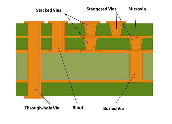
From the perspective of feature, the through-in pad can be separated right into 2 groups: One is for an electric link in between layers; the various other is for dealing with or placing tools. In regards to the procedure, these The VIP( through in pad) are normally separated right into 3 classifications, particularly blind vias, hidden vias, and also with vias. Blind vias lie on the leading as well as lower surface areas of the published motherboard as well as have a specific deepness. They are made use of to link the surface area line and also the internal line. The deepness of the hole typically does not surpass a particular proportion (aperture). Hidden opening describes the link opening situated in the internal layers of the published motherboard, which does not reach the surface area of the circuit card. The above 2 kinds of openings lie in the internal layer of the circuit card, and also are finished by a through-hole creating procedure prior to lamination, as well as a number of internal layers might be overlapped throughout the development of the by means of. The 3rd kind is called a through the opening, which passes through the whole motherboard as well as can be made use of for inner affiliation or as an element installing placing opening. Since the via opening is much easier to apply at the same time and also the expense is reduced, a lot of the published motherboard utilize it as opposed to the various other 2 kinds of through in pad.
As all of us understand, the published circuit card connecting treatment is a procedure that occurs from the greater needs to advance by the PCB production procedure as well as surface area place innovation. Its connecting features have the complying with factors:
With the advancement of digital items towards lighter, thinner, and also smaller sized, PCB has actually likewise been advertised to high-density as well as high-difficulty growth, as well as consumer demands are obtaining greater as well as greater. The demands for openings are obtaining greater as well as greater. As an example, no solder mask ink needs to get in the holes, triggering tin grains in the reds, no oil surges, as well as tough positioning of elements.
The VIP( using in pad) is an integral part of the multilayer PCB. It is not just in charge of the primary features of the PCB, however, additionally, the expense of boring normally makes up 30%-- 40% of the PCB production price.
Protect against the tin from permeating via the element surface area from through the opening to create a short circuit when the PCB is wave firm.
Prevent change deposit in the by means of.
Avoid the tin spheres from turning up throughout wave soldering, triggering short circuits.
Avoid surface area solder paste from moving right into the hole, triggering incorrect soldering as well as impacting SMT.
Via Connecting Experiment.
Exploration out the lightweight aluminum sheet that requires to be connected. The lightweight aluminum sheet is 2 inches larger than the handling board, and also the size of the hole is larger than the real handling board by 0.1 mm. Make a display or straight install it on the display printing press for connecting. After connecting the hole, it must not be parked for greater than half an hour. Usage 36T display to straight evaluate the surface area of the board. The procedure circulation is:
With this procedure, the manufacturing cycle can be much shorter, and also it can make certain that the thought openings are covered solder mask quite possibly, the plug vias are level, and also the damp movie shade corresponds. After HASL completed, it can make certain that the by means of the opening is not tinned as well as the hole does not conceal tin round, yet throughout through in pad connecting procedure, its setting is very easy to trigger oil surge after treating or hot air progressing, and also the solder mask in the red will certainly get on the pad, after that creating bad solderability.
Pierce out the lightweight aluminum sheet that requires to be connected. The lightweight aluminum sheet is 2 inches larger than the handling board, and also the size of the hole is larger than the real handling board by 0.1 mm. Make a display or install it straight on a display printing press for connecting openings. The connecting openings should be complete and also extending on both sides. It is healed as well as brightened for surface area therapy. The procedure circulation is:.
Since this procedure embraces plug opening healing to guarantee that the through the opening after HAL does not shed oil or take off, yet after HAL, it is hard to entirely address the trouble of tin round in the through opening or tin on the via the opening.
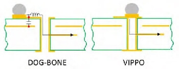
With raised intricacy of PCB styles for premium networking items, the board's densities are common> 120 mils as well as signal rates are getting to 25 GHz and also past. For these sorts of layouts, back drilling of the VIPPO frameworks ends up being critical.
Number 1 shows just how the VIPPO structure can affect those parasitical results. The signal traces, which attach the BGA pads with the vias, function as inductors. Furthermore, as high-speed layouts generally have ground aircraft promptly listed below the external layer, there is likewise a capacitive impact that is produced. With the VIPPO framework, the external trace layer is gotten rid of, consequently terminating both parasitical results.
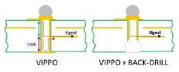
Number 2 shows the VIPPO framework as compared to the VIPPO + back drill (BD) framework. Making use of a back drill with the VIPPO structure can remove the representations within the extra section of them by means of, which works as a stub. The part of the through shown by the purple arrowhead is not in collection with the signal course, yet rather works as a stub. For that reason, a part of the signal is shown back, developing a disturbance, which will certainly break down the high-speed signal efficiency. Therefore, the objective of the back-drill is to eliminate this "extra" section of the through in order to remove the representations for a cleaner signal.
Still, need help? Contact Us: support@nextpcb.com
Need a PCB or PCBA quote? Quote now
|
Dimensions: (mm) |
|
|
Quantity: (pcs) |
|
|
Layers: |
Thickness: |
|
|
|


