
 NextPCB Capabilities
Printed Circuit Boards
NextPCB Capabilities
Printed Circuit Boards
 PCB Assembly
 Layer Buildup
 SMD-Stencils
 PCB Design-Aid & Layout
 Mechanics
 Quality
 Drills & Throughplating
 Factory & Certificate
 PCB Assembly Factory Show
Certificate
PCB Assembly Factory Show
Certificate
Support Team
Feedback:
support@nextpcb.com


For everybody that develops a PCB, eventually, they are confronted with the choice of specifying trace size. Sometimes, newbie PCB developers will just make use of the default size in the PCB format software program like Eagle, KiCad, and so on. While it mainly functions penalty for straightforward circuits, nonetheless, for circuits with a tool to high intricacy, some added elements need to be thought about. This is specifically vital when handling power circuits as well as high-frequency circuits. Choosing incorrect trace sizes might often bring about getting too hot, electromagnetic disturbances, and so on. Exceedingly big traces take in important PCB room and also boost the price of PCB. This post goes through some essential factors to consider to remember for choosing ideal trace sizes while transmitting the PCB.
For any kind of offered trace on the PCB, there is an optimum quantity of present it can manage prior to it falls short. Passing huge current via a trace will certainly create it to dissipate power as warm (like a resistor), and also offered adequate existing (and also time) the trace will certainly be ruined by either melting via, or de-laminating from the PCB thereby damaging the trace. Usually, we consider traces as no resistance attaching cords in between the elements, yet this is absolutely not the instance. All traces will certainly have some type of resistance as well as it is necessary to consider this when choosing sizes. Recognizing the resistance of a trace as well as the optimum current that will certainly be travelled through it, will certainly aid educate which size to utilize. So it is great to ask adhering to concerns prior to making a decision trace sizes:
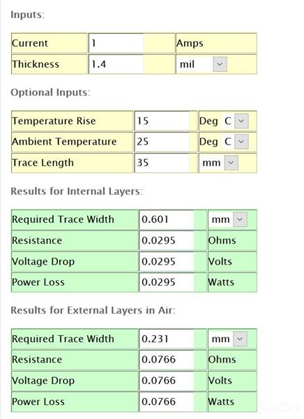
The dimension of a PCB is straight attached to the production expense of the PCB. As a result, developers intend to maintain PCBs as tiny as feasible. The drawback of minimizing board dimension is that it can restrict the readily available area to path traces. For reduced power signal traces it is usually recommended to maintain traces tiny to raise the offered area readily available for directing. Nevertheless, minimal trace size referrals from producers ought to be remembered. The minimal trace sizes as well as spacing are producer and also procedure reliant and also generally range 3mils as well as 8mils. Generally, the reduced minimum sizes often tend to be a lot more costly contrasted to greater minimal sizes. So It is suggested to prevent trace sizes less than 6mil unless it's definitely essential. The sizes of 6 to 25 mils are common for a lot of signal traces.
Occasionally, the factor at which a trace satisfies a pad can additionally educate the size of a trace. In the majority of SOIC impacts, trace sizes are readied to the exact same size as the pad they end too. This will certainly prevent breaching minimal spacing restrictions in between nearby traces. An instance situation is offered listed below:
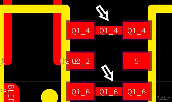
In the photo, we can see 2 traces linked to the pad of the impacts. The size of these traces is somewhat smaller sized than the size of the element pads. This enables lots of clearance in between nearby traces while directing far from the chip. Picking the trace sizes for BGA parts can be a little bit much more complicated as well as runs out of range of this write-up.
Resistance is an additional identifying consider some applications. At radio frequencies (ie. listed below a couple of MHz) insusceptibility is very little of an issue, as well as the size of the traces can be established based totally on existing handling needs or producing procedure restrictions. However, when it involves PCBs with greater regularity signals, the link on the PCB begins to act even more like a transmission line than a basic short circuit conductor. That's due to the fact that the high-frequency signal moving along the trace produces an electromagnetic field around the existing circulation, and also an electrical area (fee) in between the trace. In such instances, managed resistance is considered while making PCBs which likewise consist of trace sizes.
Still, need help? Contact Us: support@nextpcb.com
Need a PCB or PCBA quote? Quote now


 Surface

