
 NextPCB Capabilities
Printed Circuit Boards
NextPCB Capabilities
Printed Circuit Boards
 PCB Assembly
 Layer Buildup
 SMD-Stencils
 PCB Design-Aid & Layout
 Mechanics
 Quality
 Drills & Throughplating
 Factory & Certificate
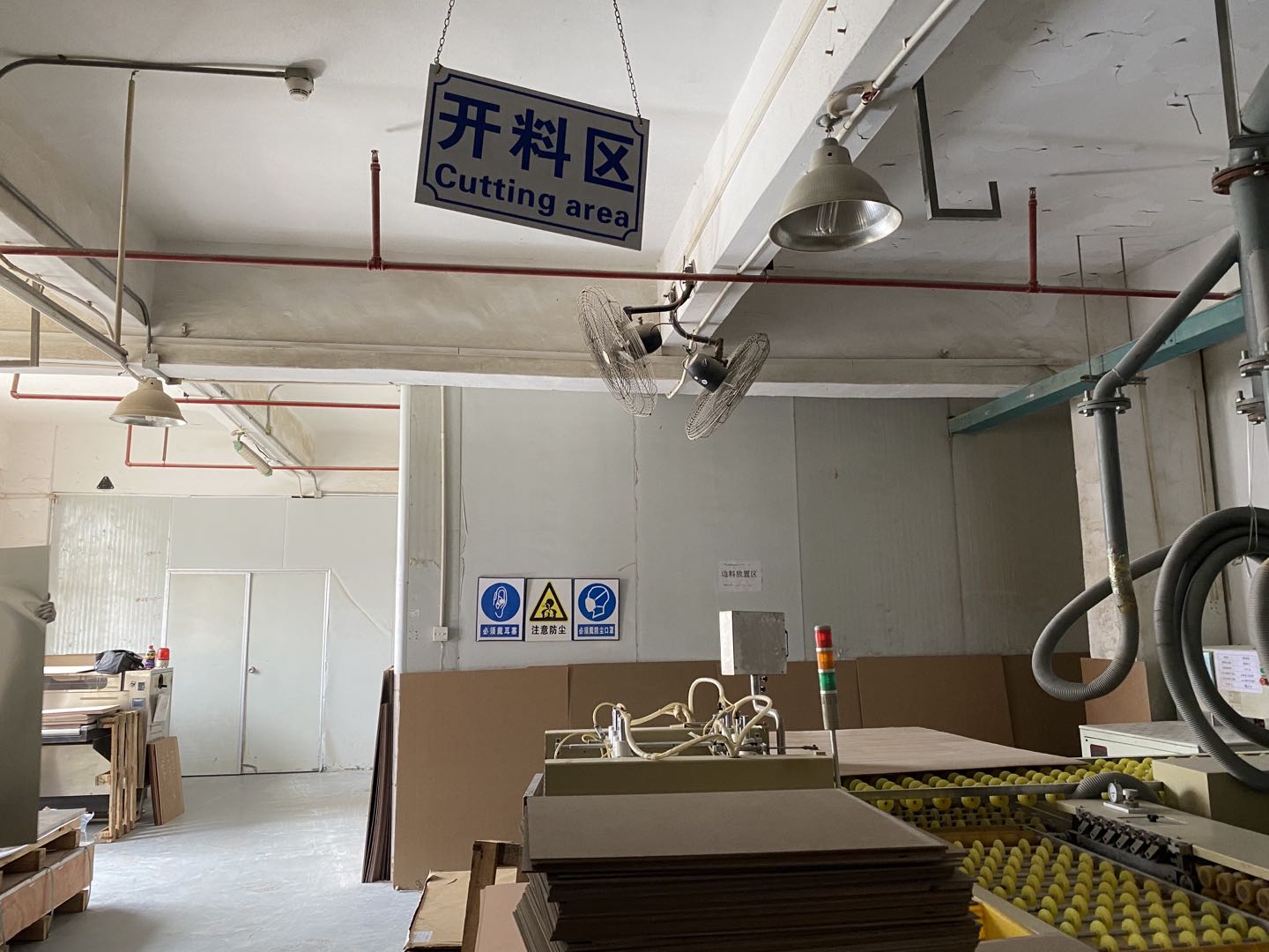
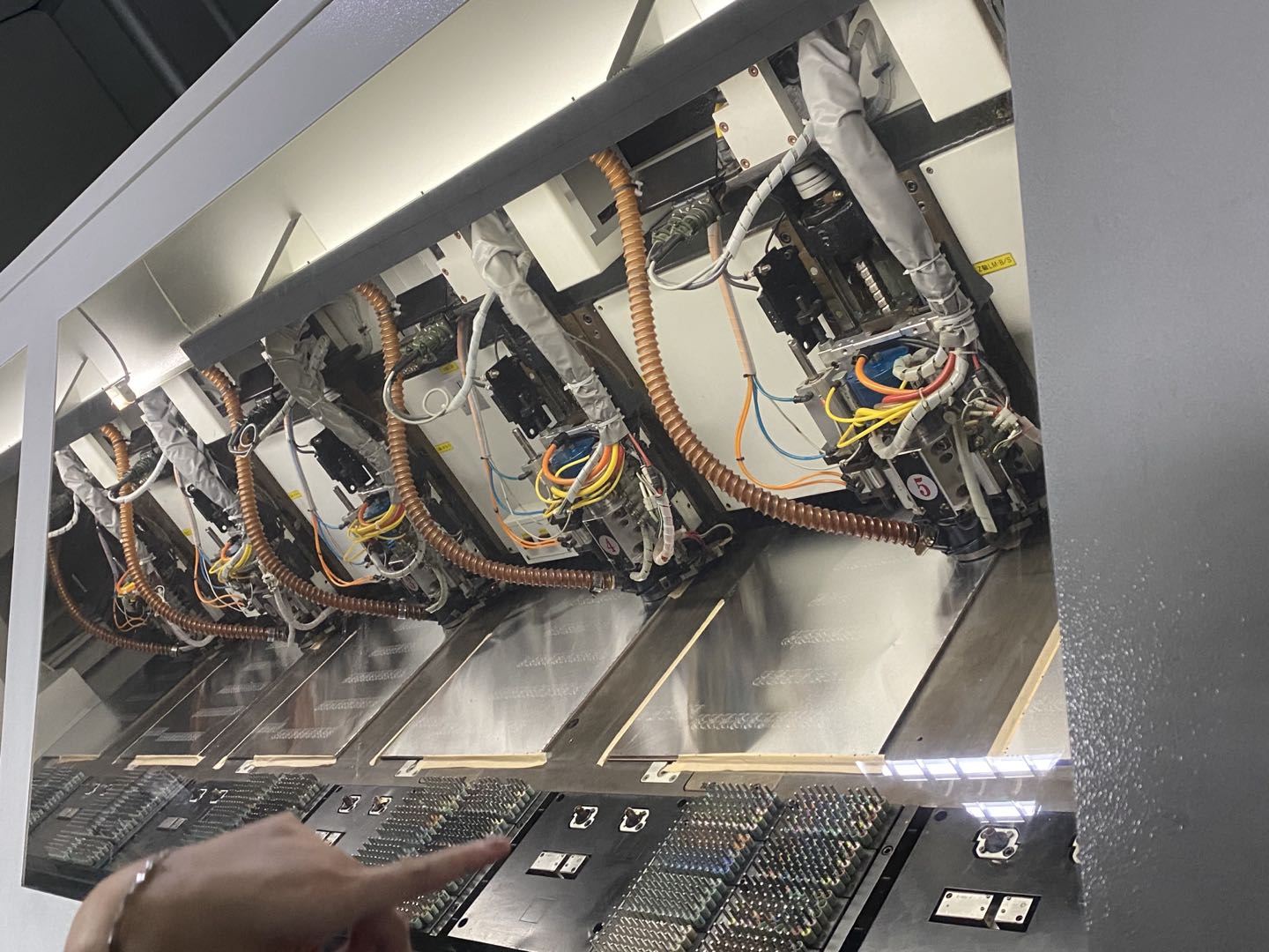
 PCB Assembly Factory Show
Certificate
PCB Assembly Factory Show
Certificate
Support Team
Feedback:
support@nextpcb.com


When the electronic devices sector from vacuum tubes, communicates the silicon semiconductor as well as an incorporated circuit when the digital parts of the dimension, as well as the rate, is decreasing. Digital items an increasing number of often shown up in the customer field, urge makers to search for smaller sized and also extra cost-efficient remedy. So, PCB birthed.
Before the development of PCB, the circuit with the incurable factor thereof. The integrity of this approach is reduced, since the circuit with aging, can cause fracture of the line interference or short circuit node. Winding innovation is a significant innovation in the circuit innovation, the technique whereby small-diameter cable injury on the post link factor, line and also to improve the toughness of interchangeability.
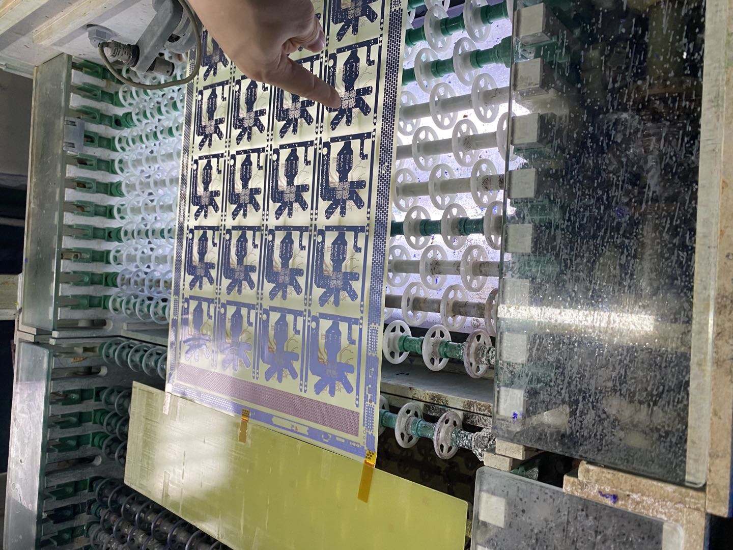
PCB manufacturing at nextpcb factory is extremely made complex to 4 PCB instance, the manufacturing procedure consists of a PCB format, making the core plate, the internal transfer PCB format, perforated core plate as well as assessment, laminating, boring, opening wall surface chemical rainfall of copper, the transfer layer PCB format, PCB layer etching action.
PCB construction and also ending up primary step is to examine the PCB design (Format). PCB manufacturing plants obtain PCB layout, CAD data since each has its very own distinct CAD software application documents layout, so the PCB manufacturing facility will certainly be changed right into a consistent style-- Extensive Gerber RS-274X or Gerber X2. After that plant designers will certainly examine the PCB format to fulfill the manufacturing procedure, there are no flaws as well as various other problems.
CCL cleansing, dirt if it can bring about the last short circuits or interference.
The number is a8-layer PCBLegend used by the 2 copper movie 3 CCL (core plate), adhered to by obstructing up the prepreg. Manufacturing order is from one of the most central of the core plates (4, 5 layer line) begins, constantly combined and afterward repaired. Manufacturing of 4-layer PCB is comparable, other than that just the core plate 2 a copper movie.
The treated photosensitive movie is torn, the subjected copper lines PCB design called for.
The dual-layer PCB format as well as movie laminates, and also ultimately put the top PCB format movie, 2 layers PCB format to guarantee specific place laminated flooring movie.
Lye and afterward treated photosensitive movie is not cleaned, the line will certainly require to be covered with aluminum foil healed photosensitive movie.
Photosensitive device photosensitive movie on a copper aluminum foil is irradiated with a UV light, the light-transmissive movie, the photosensitive movie is treated, the nontransparent movie or uncured photosensitive movie. Copper aluminum foil-covered under the treated photosensitive movie is the preferred PCB design line, representing the hand-operated activity of the printer ink PCB.
Initially to develop one of the most intermediate core plates (Core) of both lines. It will certainly be covered with a layer externally of the photosensitive movie CCL tidy. Such light might come across the movie is healed to create a safety movie on the copper aluminum foil copper-clad laminate.
After that with a solid base, such as NaOH etching away undesirable copper aluminum foil.
The Core board has been efficiently created. After that struck placement openings in the core plate, as well as various other products to help with succeeding positioning. As soon as the core plate and also the various other PCB layers are compressed, it can not be changed, so the check is necessary. Instantly as well as PCB design illustrations for contrast by the equipment, see the mistake.
The PCB board is secured iron plates were put on the cradle, and afterward sent out to a vacuum cleaner warm press lamination. Vacuum cleaner warm pushing equipment in heat can thaw the epoxy material in the prepreg sheet, the core plates are under pressure as well as a copper aluminum foil is safeguarded with each other.
After lamination is total, eliminate the top layer of the PCB pushing iron. The stress was after that eliminated lightweight aluminum, lightweight aluminum additionally operates to separate various PCB and also PCB make certain smooth external copper aluminum foil obligation. In this situation is covered by a smooth layer of copper aluminum foil on both sides runs out the PCB.
It needs to be a brand-new product called a prepreg, with (4 PCB layers >), and also a glue layer in between the core plate and also the core plate copper core plate, as well as likewise works as insulation.
Reduced copper aluminum foil and also a prepreg has 2 set placements beforehand via the placement opening and also a reduced iron plate, as well as likewise make a great core plate placement opening right into the last turn prepreg layers, as well as a layer of copper aluminum foil layer under pressure onto a lightweight aluminum plate covered with the core plate.
By X-ray drill device is placed on the internal core plate, the equipment will instantly discover as well as placing openings on the core plate, and also a significant PCB placing openings, guarantee that boring is complied with from the facility via the hole as well.
To PCB in the copper aluminum foil layer, 4 are collaborated without getting in touch with, the initial to be pierced up and down with the openings to open the PCB, as well as the hole wall surface by conductive metallization.
Before the lamination action, the dissolved epoxy material is squeezed out to the outdoors PCB, so the demand for elimination. Camera milling device for reducing the outer PCB according to its correct XY collaborates.
A layer of lightweight aluminum on the strike device, after that put on top of the PCB. To enhance performance, according to a PCB layers 1 to 3 will certainly coincide with PCB board piled perforated. Lastly, a lightweight aluminum plate covered with a layer of the PCB on the uppermost, top as well as reduced degrees of lightweight aluminum to boring when the drill little bit and also the pierced copper aluminum foil without tearing the PCB.
Given that nearly all PCB styles are perforated lines to link various layers, a great link needs 25 microns copper movie on the wall surface of the hole. The density of this copper movie by electroplating requirements to attain, however, the cell wall surfaces are non-conductive epoxy material and also glass fiber structure.
So the primary step is the very first layer of conductive product transferred on the pore wall surfaces, chemically transferred over the whole surface area of the PCB fashion, additionally making up a copper movie is based on the pore wall surfaces 1 micron. The entire procedure such as chemical therapy and so forth are cleansed by the maker control.
The following layer will certainly be moved to the PCB design of a copper aluminum foil of an internal layer plate procedure as well as before the PCB design concept of transfer are comparable copy making use of the photosensitive movie as well as the movie PCB format moved to the copper aluminum foil just distinction is that will certainly be made use of to make favorable plates.
Transfer layer PCB design is generally made use of technique, utilizing favorable plates do. The treated photosensitive movie is covered with a non-circuit location on the PCB. After layering the treated photosensitive movie is not cleaned. At layering, a movie can not have, yet not at the membrane layer, after the very first layering tin-plated copper. Removing after antacids engraving, and also ultimately handed down in. Line graphics since the tin safeguarded left on the board.
The PCB with clips, electroplated copper. As discussed previously, to guarantee enough opening excellent electric conductivity, the hole wall surfaces layered copper movie have to have a density of 25 microns, to ensure that the whole system will certainly be instantly managed by a computer system, to guarantee its precision.
Moving the internal layer PCB design subtractive approach is utilized, we make use of an adverse plate made. The treated photosensitive movie is covered on a PCB circuit, not cleaned off the treated photosensitive movie is subjected after the copper aluminum foil is engraved, PCB format line is safeguarded by the treated photosensitive movie to leave.
Next, the etching procedure is done by an entirely automated production line. Initially, the PCB treated photosensitive movie is cleaned. The copper aluminum foil is after that cleaned undesirable covering with a solid base. And after that removing remedy of tin plating on the copper removing PCB design. After tidy 4 layer PCB format is full.
Still, need help? Contact Us: support@nextpcb.com
Need a PCB or PCBA quote? Quote now


 Surface

