In the last article, we have introduced “ What is PCB and Types of PCB?” and I believe we can not say it again. Next, let’s learn something new. Most of the students majoring in electronic engineering need to try to make simple electronic circuit DIY projects and make PCBs. This article will introduce "how to make PCB at home" without any special materials. Let’s briefly review the content of the previous article.
PCB Introduction
PCB: The full name is printed circuit board, which is the support of electronic components and the carrier of the connection of electronic components. PCB types can be divided into single-layer PCB, double-layer PCB, multilayer PCB, rigid PCB, high-frequency PCB, flexible PCB, rigid-flexible PCB, aluminum backplane, and other types.
Three Ways to make PCB at home
cut copper-clad board into a circuit diagram
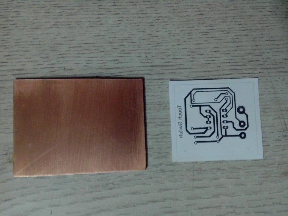
- 1. Cut the copper-clad board to the size required by the circuit diagram.
- 2. Put the wax paper on the steel plate, use a pen to engrave the circuit diagram on the wax paper 1:1, and cut the circuit diagram engraved on the wax paper according to the size of the circuit board, and place the cut wax paper on the printed copper board. Take a small amount of paint and talcum powder to make a suitable thin and thick printing material, dip the printing material with a brush, and evenly apply it to wax paper, repeat it several times, and the circuit can be printed on the printed board. This kind of stereotype can be used repeatedly and is suitable for small batch production.
- 3. Use 1 gram of potassium chlorate and 40 milliliters of 15% hydrochloric acid to prepare a corrosive solution, and apply it to the corroded area on the circuit board for corrosion.
- 4. Wash the corroded printed board with water repeatedly. Wipe off the paint with banana water, and then wash it several times to make the printed board clean without leaving corrosive liquid. Apply a layer of rosin solution and let it dry before drilling holes.
Making printed boards under amateur conditions
There are many ways to make printed boards under amateur conditions, but they are either time-consuming, complicated in "workmanship", or uncomfortable in quality. And my method of making printing plates is one of the better comprehensive effects, the method is as follows:
- 1. Printed board map. The pads in the figure are represented by dots, and the connection can be a single line, but the position and size must be accurate.
- 2. Cut the printed board according to the size of the printed board drawing, and clean the copper foil surface.
- 3. Use carbon paper to copy the diagram to the printed board. If the circuit is simple and the producer has a certain board-making experience, this step can be omitted.
- 4. According to the actual situation of the component, paste the standard pre-cut symbols (pads) with different inner and outer diameters; then paste the tape lines of different widths depending on the current. Standard pre-cut symbols and tape are available in electronic stores. The common specifications of pre-cut symbols are D373 (0D-2.79, ID-0.79), D266 (0D-2.00, ID-0.80), D237 (OD-3.50, ID-1.50), etc. It is best to buy paper-based materials. (Black), plastic-based (red) materials should not be used as much as possible. The commonly used specifications of tape are 0.3, 0.9, 1.8, 2.3, 3.7, etc. The units are all millimeters.
- 5. Use a softer hammer, such as smooth rubber, plastic, etc. to hit the sticker to make it fully adhere to the copper foil. Focus on the bend and overlap of the line. When it is cold, it is best to use a heater to increase the surface by.
- 6. It is corroded by adding ferric chloride, but it should be noted that the liquid temperature is not higher than 40 degrees. After corrosion, it should be taken out and rinsed in time, especially if there are thin lines.
- 7. Drill the eyes, polish the copper foil with fine sandpaper, apply rosin alcohol solution, and let it dry to complete the production. The quality of this type of printed board is very close to the distance of the printed board. The 0.3mm tape can pass between the IC legs, but I often use this method to make experimental printing plates or small amounts of products in my work.
PCB Design Analysis Software-NextDFM One-click Design Analysis for Manufacturability

"Sub-printing'method to make printed circuit boards
Radio enthusiasts have bothered to make circuit boards. Now I will introduce a kind of "sub-printing" method to make printed circuit boards. Methods as below:
1. Print the circuit board diagram on the printer at a ratio of 1:1 on 80 grams of copy paper. Hand-drawing is also possible, but the bottom paper should be flat.
2. Find a fax machine, take out the fax paper from the machine, and replace it with a hot-melt plastic film (sold by our company). Put the circuit diagram into the entrance of the fax machine, and use the copy button of the fax machine to copy the circuit diagram on the hot-melt plastic film. At this time, the "printed manuscript" of the printed circuit board is ready.
3. Use double-sided adhesive tape to affix the painted plastic film to the copper-clad board evenly. Pay attention to be flat, not wrinkle, tape paper can not cover the melted part, otherwise, it will affect the production effect of the circuit board.
4. Use a paintbrush to evenly brush the paint on the plastic film. Note: Do not brush back and forth, only brush in one direction, otherwise the plastic film will wrinkle together and the lines on the copper plate will overlap. After the circuit diagrams have been brushed all over, carefully remove the plastic film. At this time, a printed circuit board is printed. After it dries, it can be corroded.
If you want to print more than one piece, you can make a wooden frame larger than the circuit board, and lay the screen (the company sells it) on the wooden frame evenly, and fix it. Then use double-sided tape to stick the fixed plastic film under the screen. Put the copper-clad board on the table, close the screen frame (the printed picture and the copper-clad board should be aligned left and right), use a paintbrush to paint in one direction, and remove the screen frame. The printed circuit board is printed. If there is any defect, it can be modified with paint and bamboo.
Pay attention to the above process. When painting, the hand force should be light and heavy. If the paint film is too heavy, the lines will run out of lace, and the lines will break if they are too light. The plastic film must face up.

 NextPCB Capabilities
 PCB Assembly
 Layer Buildup
 SMD-Stencils
 PCB Design-Aid & Layout
 Mechanics
 Quality
 Drills & Throughplating
 Factory & Certificate
 PCB Assembly Factory Show
Certificate
PCB Assembly Factory Show
Certificate


 Surface

