
 NextPCB Capabilities
Printed Circuit Boards
NextPCB Capabilities
Printed Circuit Boards
 PCB Assembly
 Layer Buildup
 SMD-Stencils
 PCB Design-Aid & Layout
 Mechanics
 Quality
 Drills & Throughplating
 Factory & Certificate
 PCB Assembly Factory Show
Certificate
PCB Assembly Factory Show
Certificate
Support Team
Feedback:
support@nextpcb.com


Layout is one of the most basic job skills for PCB design engineers. The quality of the wiring will directly affect the performance of the entire system. Most high-speed design theories are finally realized and verified through Layout. It can be seen that wiring is crucial in high-speed PCB design. The following will analyze the rationality of some situations that may be encountered in actual wiring, and give some more optimized routing strategies. It is mainly explained from three aspects: right-angle wiring, differential wiring, and serpentine wiring.
Right-angle wiring is generally a situation that needs to be avoided in PCB wiring as much as possible, and it has almost become one of the standards for measuring the quality of wiring. So how much influence will the right-angle wiring have on signal transmission? In principle, right-angle routing will change the line width of the transmission line, causing discontinuity in impedance.
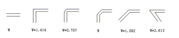
Not only right-angled wiring, but also corners, sharp-angled wiring may cause impedance changes. The influence of the right-angle wiring on the signal is mainly reflected in three aspects:
C=61W(Er)1/2/Z0
In the above formula, C refers to the equivalent capacitance of the corner (unit: pF), W refers to the width of the trace (unit: inch), εr refers to the dielectric constant of the medium, and Z0 is the characteristic impedance of the transmission line. For example, for a 4Mils 50 ohm transmission line (εr is 4.3), a right angle brings
The capacitance is about 0.0101pF, and then the rise time change caused by this can be estimated:
T10-90%=2.2*C*Z0/2 = 2.2*0.0101*50/2 = 0.556ps
It can be seen through calculation that the capacitance effect brought by the right-angle trace is extremely small.
As the line width of the right-angle trace increases, the impedance there will decrease, so a certain signal reflection phenomenon will occur. We can calculate the equivalent impedance after the line width increases according to the impedance calculation formula mentioned in the transmission line chapter, and then Calculate the reflection coefficient according to the empirical formula:
ρ=(Zs-Z0)/(Zs+Z0)
Generally, the impedance change caused by right-angle wiring is between 7%-20%, so the maximum reflection coefficient is about 0.1. Moreover, as can be seen from the figure below, in W/2.
The impedance of the transmission line changes to the minimum within a long line, and then returns to the normal impedance after W/2 time. The entire impedance change time is extremely short, often within 10ps. Such fast and small changes are very important for general signal transmission. It is almost negligible.
Many people have this understanding of right-angle wiring. They think that the tip is easy to transmit or receive electromagnetic waves and generate EMI. This has become one of the reasons why many people think that right-angle wiring cannot be used. However, many actual test results show that right-angled traces will not produce more obvious EMI than straight lines. Perhaps the current instrument performance and test level restrict the accuracy of the test, but at least it illustrates a problem. The radiation of the right-angled wiring is already smaller than the measurement error of the instrument itself.
In general, right-angle routing is not as terrible as you imagined. At least in applications below GHz, any effects such as capacitance, reflection, EMI, etc. are hardly reflected in TDR testing. High-speed PCB design engineers should still focus on layout, power/ground design, and wiring design. Other aspects such as vias. Of course, although the impact of right-angle wiring is not very serious, it does not mean that we can use right-angle wiring in the future. Attention to detail is the basic quality that every good engineer must have. Moreover, with the rapid development of digital circuits, PCB The frequency of signals processed by engineers will continue to increase. In the RF design field above 10GHz, these small right angles may become the focus of high-speed problems.
Differential signals are more and more widely used in high-speed circuit design. The most critical signals in circuits are often designed with differential structures. Why is it popular? How to ensure its good performance in PCB design? With these two questions, we proceed to the next part of the discussion.
What is a differential signal? In layman's terms, the driving end sends two equal and inverted signals, and the receiving end judges the logical state "0" or "1" by comparing the difference between the two voltages. The pair of traces carrying differential signals is called differential traces.
Compared with ordinary single-ended signal traces, differential signals have the most obvious advantages in the following three aspects:
Snake line is a type of routing method often used in Layout. Its main purpose is to adjust the delay to meet the system timing design requirements. The designer must first have this understanding: the serpentine line will destroy the signal quality, change the transmission delay, and try to avoid using it when wiring. However, in actual design, in order to ensure that the signal has sufficient hold time, or to reduce the time offset between the same group of signals, it is often necessary to deliberately wind the wire.
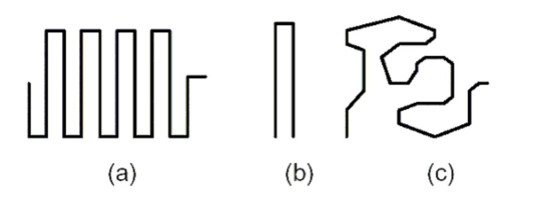
When the signal is transmitted on the serpentine trace, there will be coupling between the parallel line segments.In the form of differential mode, the smaller the S and the larger the Lp, the greater the degree of coupling. It may lead to a reduction in transmission delay, and greatly reduce the quality of the signal due to crosstalk.
Still, need help? Contact Us: support@nextpcb.com
Need a PCB or PCBA quote? Quote now


 Surface

