
 NextPCB Capabilities
Printed Circuit Boards
NextPCB Capabilities
Printed Circuit Boards
 PCB Assembly
 Layer Buildup
 SMD-Stencils
 PCB Design-Aid & Layout
 Mechanics
 Quality
 Drills & Throughplating
 Factory & Certificate
 PCB Assembly Factory Show
Certificate
PCB Assembly Factory Show
Certificate
Support Team
Feedback:
support@nextpcb.com


The significance of electromagnetic compatibility (EMC) of electronic circuits and systems has recently been increasing. This increase has led to more stringent requirements for the electromagnetic properties of equipment. Two property aspects are of interest: the ability of a circuit to generate the lowest (or zero) interference, and the immunity of a circuit to the effects of the electromagnetic energy it is subjected to. The effects on electronic circuits and systems are well documented, but little attention has been paid to circuit behavior and the interference it generates. This application report explains important criteria that determine the EMC of a circuit and, thus, provides the development engineer with information for the design of circuits and layout of circuit boards.
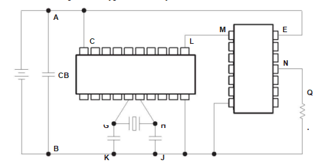
The EMC of an electronic circuit is mainly determined by how components are laid out with respect to each other and by how electrical connections are made between components. Every current flowing in a line generates a current of the same magnitude flowing in a corresponding return line. This line loop creates an antenna that can radiate electromagnetic energy whose magnitude is determined by the current amplitude, the repetition frequency of the signal, and the geometrical area of the current loops. Figure 1 shows the current paths of a typical circuit layout.
Classes of lines that contribute, in varying degrees, to the undesirable radiation that is generated are:
Knowing the relationships of several important properties of logic circuits leads to specific and effective ways of improving EMC. These properties are demonstrated with CMOS integrated circuits (ICs). An example will help explain several improving effects that arise in a similar way with other device technologies.
Figure 2 shows the circuit of a simple inverter constructed with N-channel and P-channel transistors. If a voltage, VI, is applied to the input, which is less than the threshold voltage (VIT–) of the N-channel transistor, this transistor will be nonconducting, whereas, the P-channel transistor will conduct. In the opposite way, the N-channel transistor will conduct and the P-channel transistor will be nonconducting if a voltage VI > VCC – VIT+ is applied at the input (VIT+ is the threshold voltage of the P-channel transistor). In both cases, no current, except negligible leakage currents, flows through the circuit. This is also the reason for the extremely low current consumption of CMOS circuits in a quiescent state.
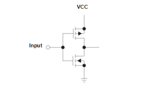
However, if a voltage between the two limits (VIT and VCC – VIT ) is applied to the input of this inverter, both transistors will be more or less conducting. The result with this configuration is a considerable increase in the supply current (see Figure 3). In such a case, HCMOS circuits take a current of up to about 1 mA, whereas, with advanced CMOS (AC), the supply current can increase to over 5 mA.
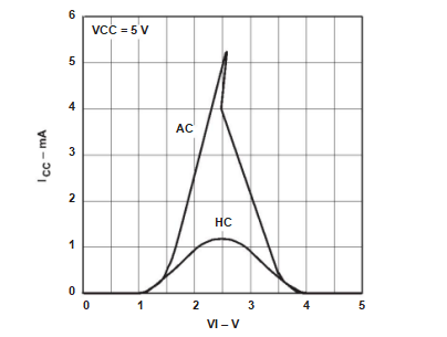
Because the input voltage at such a circuit cannot traverse the critical voltage region when changing from a low to a high (or vice versa) in an infinitely short time, there is flow during this time of pulse-shaped current peaks (often known as current spikes), of such magnitude that cannot be neglected. In an input stage, current amplitudes of 1 mA to 5 mA must be expected (see Figure 3). Considerably more critical is this phenomenon at the outputs of an IC. Since the output stages must drive the load that is connected to the output, these transistors must be made considerably bigger. As a result, the amplitudes of the current peaks also increase correspondingly to values of from 20 mA for HCMOS devices to 60 mA for AC devices, with a pulse width of 5 ns to 10 ns.
The current peaks mentioned previously are one of the most significant causes of electromagnetic interference. Every time output is switched, a corresponding pulse of current flows along the supply lines. The latter connections lead by a more or less direct route from the module to the central power supply. The problem will be aggravated when the outputs of an IC are switched at a high repetition rate, such as along the lines connecting a processor with its corresponding memory.
In practice, decoupling the supply voltage close to the IC with a ceramic capacitor (CB = 100 nF) is recommended. In digital systems, this technique is effective in ensuring that, with the expected load changes, no inadmissible supply voltage changes can occur. However, this will result in only a very limited reduction of electromagnetic interference.
To achieve a significant improvement, it is first necessary to analyze the complete circuit and its parasitic components. Figure 4 shows the circuit under examination. Two transistors (Q1 and Q2) are the output stage of an IC whose behavior is to be analyzed. Connection to the surrounding circuitry is made with the Lp/Rp/Cp network, which represents the parasitic components of the package. The following individual values are assumed:
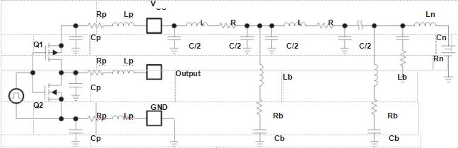
From the supply terminals VCC and GND of the IC, a connection is made to CB as identified in Figure 1 across the dc source. The following values for the components of the impedance per unit of length of the line from the VCC source on the circuit boards to the VCC terminal of the IC are assumed:
The supply line subsequently reaches the first blocking capacitor, CB (see Figure 4, right-hand Lb, Rb, Cb totem), whose equivalent circuit is made up as follows:
From here, a long line (length = 5 cm) is taken to the next blocking capacitor, CB (see Figure 4, center Lb, Rb, Cb totem); this line and the capacitor can also be represented by the same equivalent circuit as mentioned above. For simplicity, it will be assumed that the subsequent circuit can be represented by the well-known vehicle power-supply equivalent circuit components:
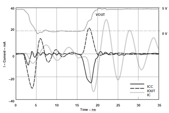
The behavior of this circuit was simulated using a SPICE program; it was assumed that no load was connected to the output of the IC, i.e., the circuit was left open. Figure 5 shows the calculated current waveforms. The following definitions apply:
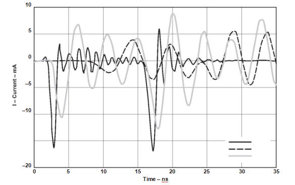
The waveform of the current ICC demonstrates the current peaks already mentioned that have an amplitude of about 15 mA.
From the previous discussion it can be determined that the blocking capacitor is now scarcely able to smooth out this pulse of current. In fact, the resonant circuit formed by the line inductance (principally that of the package of the IC) and the CB will be excited, and an increase of current will take place (current IC1). A major part of the current (IC2) is transplanted via the supply line and flows with a scarcely diminished amplitude also into the next CB.
From the point of view of the EMC of the circuit shown, CB, in this form, is unable to significantly reduce the radiated interference. The long supply lines – which, in practice, are always present – with the relatively large areas that these lines surround, form an effective antenna. At the frequencies present, an unacceptable level of interference is radiated.
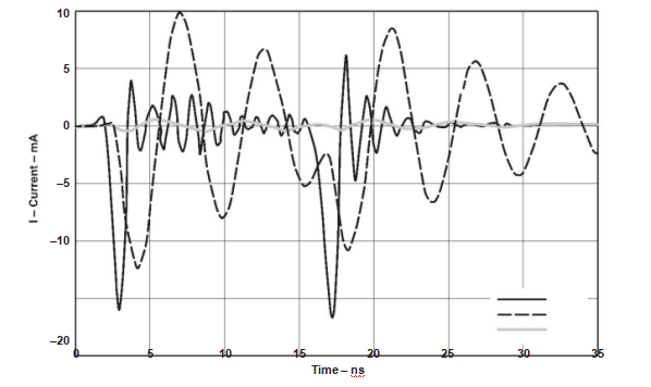
To improve the behavior of the circuit, measures must first be taken to ensure that the spread in the system of the currents shown in Figure 5 is limited. This cannot be achieved with CB alone; improvement of its properties, relative to the requirements detailed here, cannot be achieved. Because the inductance causing the interference has already been formed, to a large extent by the packages of the ICs and by the connection to the capacitor, no significant improvement can be achieved by simply connecting in parallel several capacitors having different capacitance values. Of greater concern is preventing the current causing the disturbance from reaching other parts of the circuit. This can be achieved by introducing an inductive coil behind the first CB, which represents a sufficiently high resistance at high frequencies. In the simulated circuit, an inductor having an inductance LCH = 1 µH was assumed, the impedance of which could be limited at high frequencies by a resistor of 50 Ω connected in parallel.
The results of the simulation are shown in Figure 6. As might be expected, the currents in the leads to the IC ICC and in the first CB (IC1) have not become any smaller. However, Figure 6 shows that there is a reduction of the current amplitude (ICH) by more than 20 dB after the inductor. This method can contribute to a significant reduction of the radiation.
Next is the question of how the individual components should be arranged on the circuit board to achieve the maximum reduction of the radiation. Figure 7 shows a circuit proposal for this purpose. A grounded area under the IC is connected to the GND pin of the circuit. This ground ensures that the major part of the field lines emanating from the IC is concentrated between the IC and ground level. As a result of the skin effect on the large surface area, the line inductance to CB is reduced still further. It is immaterial whether the capacitor is situated near the positive (VCC) or the negative (GND) supply connection.
It is only important that the parasitic inductances and the effective areas of the antennas are kept as small as possible. The inductor (LCH) should be as close as possible to the part of the circuit where the interference is to be suppressed.
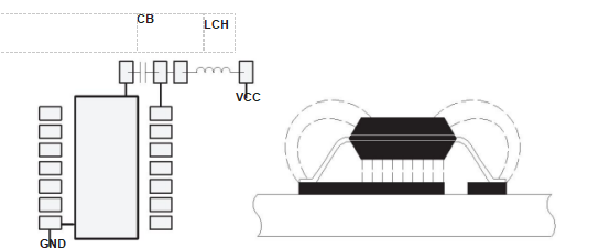
Figure 8 shows where the signal currents should flow to reduce the interference radiated from the signal lines. In this circuit, a gate drives a line that is terminated with an impedance Z. The impedance can be made up of the IC input capacitance (CIN = 5 pF) and its input resistance (RIN) of several kilohms to a few megohms. At the transmission of a negative signal edge, the current flows from the output of the driver to the drain, and from the drain, via the ground line, back to the signal source. Simply expressed, the capacitance of the connecting line and the input capacitance of the receiver are discharged via the output resistance of the driver. When a positive signal edge is transmitted, the opposite occurs: this capacitance must be charged by the supply voltage source via the output resistance of the driver. In this case, these signal currents also appear on the supply lines. This demonstrates that the precautions taken to reduce interference from the supply lines are effective.
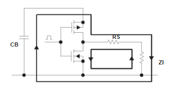
Figure 9 shows the results of the simulation of the arrangement just discussed. In this example, the output of the IC drives a 5-cm-long line having a characteristic impedance (ZO = 100 Ω) that is terminated at its end with 100 kΩ and 5 pF in parallel. As a result of the largely capacitive loading, the amplitude of the current peak ICC is significantly reduced on the negative edge at the output VOUT. The capacitance at the output keeps the voltage at this point at the original potential (high) for a short time and prevents a current flow through the upper transistor of the output stage (voltage difference = 0 V). At the positive edge, the signal current IOUT is added to the lateral current in the output ICC.
Currents may be reduced by connecting a resistance (RS) in series with the output. Line-transmission theory shows that this resistance has no negative influence on the speed of the circuit, provided the output resistance of the driver (consisting of its internal resistance + series-resistance RS) is smaller than, or equal to, the characteristic impedance of the line (ZO = 70 Ω to120 Ω) to which it is connected. In practice, resistance values are about 50 Ω, so the current amplitude can be reduced by about 3 dB. This solution needs more components and should be used only when the distortion resulting from line reflections must
be reduced at the same time.
Care should be taken to make the antennas as ineffective as possible, i.e., make the areas enclosed by the outward and return lines as small as possible. An effective method is to run the return line parallel to the signal line (see Figure 10). (This is automatically ensured with multilayer circuit boards that have a continuous ground level under the signal lines.) If signals with high frequencies (such as clock signals) are transmitted or lines are very long, this method will often be used. In this case, lines having defined line impedances (be cautious of reflections) as a result will also be provided. With an appropriate layout of the additional ground lines, crosstalk between critical lines can be reduced.
The most cost-effective and technically-effective method consists simply of keeping the critical lines as short as possible, while observing the following priorities:
All ICs between which information at high frequencies is exchanged should be mounted as close to one another as possible to keep the line lengths short. This applies particularly to lines between a microprocessor and its memory.
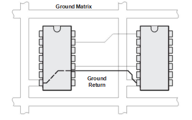
The next step is to keep the areas of the antennas as small as possible, i.e., to provide the transmitted signals with a return path which, in turn, is as close as possible to the corresponding signal line. To reduce the effect of tangled lines on circuit boards for fast digital circuits, a ground connection of the circuit board in the form of a network is effective, but the mesh area should be only a few square centimeters. In this way, the inductance of the connections to ground and their lengths can be optimized.
This technique results in short return lines and in small-area antennas. With a logical reduction of the mesh area, a final arrangement conforms electrically to that of a continuous ground layer in a multilayer circuit board. Ground lines with a spacing of 2 cm to 4 cm horizontally and vertically make up the required network structure. Subsequently, all free areas can be filled out with copper, which then must be connected by the shortest possible path to ground potential. With large areas, it is advisable to make the contacts at several of the ends. With the positive supply line connected firmly to the supply-voltage connections via the blocking capacitors to the ground system, a network structure connection is not needed.
The highest frequencies in digital systems are usually found in the clock generator. From this point, the oscillator signal is transmitted to the other subsystems, mostly in the form of a divided frequency. It is customary for the oscillator amplifier to be integrated into the microcomputer or processors so that only passive components, such as the crystal and necessary capacitors, need to be connected externally (see Figure 11).
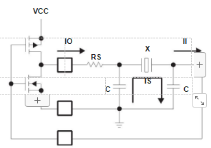
The crystal-oscillator circuit needs to be analyzed with respect to the flow of significant currents to determine where interference suppression is necessary. A parallel resonant circuit is formed by the delta section, consisting of the crystal (X) and the two capacitors (C). The crystal behaves like an inductance, with the resonant frequency being somewhat above the actual resonant frequency of the crystal. The impedance of the delta section, measured at the input or output, typically amounts to several tens of kilohms because of the high Q of the crystal. When components are correctly dimensioned, a very small current (IO) flows between the amplifier and the external components because of the high resistance of the circuit.
However, there is an opposite effect as a result of the MOS circuits not having output impedances that are ideally matched to the crystal; they should also be several kilohms. In addition, these circuits usually supply a square-wave signal containing harmonics, to which the delta section no longer represents a high resistance. The result is correspondingly high output currents in the amplifier. An improvement usually can be achieved by a resistor (RS) in series with the amplifier output (see Figure 11). Ideally, the voltage waveform at the input of the resonant circuit will then be a sine wave. The output is correctly terminated by the high input impedance of the MOS circuit, such that, in this case, only a very small current (II) flows. Capacitor C (see Figure 11) has an impedance of only a few hundred ohms at the resonant frequency. Consequently, a current (IS) flows in the resonant circuit that is much higher than the current on the line leading to this part of the circuit. This loop must be regarded as considerably more critical; therefore, construction must be compact, with extremely short lines.
Figure 12 suggests how this can be done. The two capacitors (C) of the resonant circuit are placed directly beside the crystal (X). Note that these components should be as close as possible to the corresponding pins of the IC.
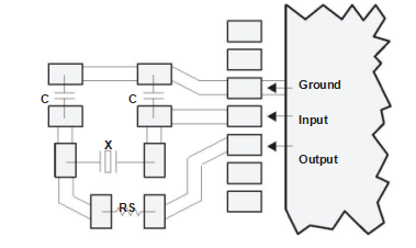
The crystal and the capacitors’ part of the circuit board, and the radiated interference that results from them, are largely under the control of the development engineer. Nevertheless, it is also necessary that the ground connection needed for the amplifier be made as near as possible to the IC, i.e., besides the amplifier connections, if possible. This ensures that when there are also longer connections in the IC package, unavoidable current loops will enclose only a small area.
This application report covers several important factors to be considered when designing circuit boards to ensure the EMC of subsystems. The proposals are based on well-understood basic principles and have been successfully implemented to make electronic circuits immune to self-generated interference (e.g., crosstalk) or interference coupled into them from outside sources. Since radiation is simply the opposite of irradiation, the logical further development and application of these rules result in circuits that fulfill the requirements of electromagnetic compatibility.
The implementation of EMC-compatible circuit boards begins when a circuit is first being developed and components are being selected. If wrong decisions are made at this early stage, they often must be corrected later with a considerable expenditure in time and effort, for example, with costly screening. An understanding of circuit operation is absolutely necessary when laying out circuit boards to ensure that appropriate ECM measures are taken. The reduction of the effective areas of the antennas requires, for example, that not only the signal line is taken by the shortest route, but the corresponding return line as well. Perhaps a longer line, but one that is taken parallel to an existing ground or supply line will be the better solution. Computer-aided layout programs have, until now, been unable to provide useable results with respect to an improvement in EMC. The processes used for these programs do not take electrical requirements into account. This means that the experience of the development engineer is needed to decide how and where every critical connection should be made. The computer can then serve as an intelligent draftsman.
This report is from TI.
Still, need help? Contact Us: support@nextpcb.com
Need a PCB or PCBA quote? Quote now


 Surface

