
 NextPCB Capabilities
Printed Circuit Boards
NextPCB Capabilities
Printed Circuit Boards
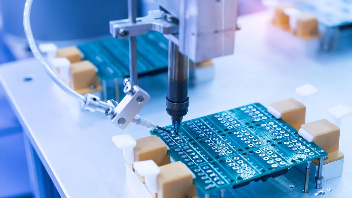
 PCB Assembly
 Layer Buildup
 SMD-Stencils
 PCB Design-Aid & Layout
 Mechanics
 Quality
 Drills & Throughplating
 Factory & Certificate
 PCB Assembly Factory Show
Certificate
PCB Assembly Factory Show
Certificate
Support Team
Feedback:
support@nextpcb.com


PCB has been playing a major role in electronics today. It is the primary part of any electronic component. Thus, the major concern is PCB quality, which is crucial, without a doubt. Optimal and accurate PCB design requires following guidelines and standards when considering the world of PCB design. Testing and simulating the product is still necessary to ensure that it performs as intended over a specified period and is reliable. It is necessary to perform these tests to assess the PCB's performance, reliability, and accuracy. The quality of PCB is inspected through various reliability tests. This article provides all the required and important PCB reliability test, their test principles, and their processes.
Schematics and hardware designs are the starting point for reliability tests. It is based on the properties of components and their placement in circuit designs.
This test checks the potential issues of the solder joint, functionality issues, and short circuits of the board. All the PCB test helps to improve the reliability of the PCB and also helps to improve the functionality and design of the PCB.
Overall, the reliability test offers various benefits:
The solder Mask Hardness test is one of the quality control tests on PCB. It determines the adhesion and hardness of the solder mask layer. This testing is important because the solder mask layer protects the PCB traces. It then prevents solder bridges from forming between adjacent components during the soldering process.
This testing aims to ensure that the solder mask is hard enough. The poor solder mask layer can crack off during the operation and lead to electrical failures.
The test principle involves applying controlled pressure to a small area of the solder mask layer using a hardness test pen. The hardness tester measures the resistance of the solder mask layer to indentation and deformation. It indicates the hardness and adhesion strength of the layer. The standard test pencil hardness grade is ordered as follows:
4B>3B>2B>B>HB>F>H>2H>3H>4H>5H>6H
The minimum harness for this solder mask testing should be greater than 6H.
The basic testing process of this hardness test includes the following:
This reliability test is performed on electronic assemblies that erect the presence of ionic contaminants. The presence of ions can impact the reliability and performance of the assembly. The major purpose of this test is to ensure the board is free from ionic contaminations, as it can cause electrical shorts, corrosion, and many other failures.
It is tested through an Ion pollution machine: By detecting the number of ions per unit surface area of the sample, it can be judged whether the cleanliness of the sample meets the requirements.
The test principle involves immersing the electronic assembly in a test solution that dissolves any ionic contaminants present on the surface. The contaminants are then transferred to the test solution, and their concentration is measured using a conductivity meter or ion chromatography. The results are compared to specified acceptance criteria. It then determines whether the assembly meets the required level of cleanliness.
The criteria for this ionic test is that the ion concentration should be 6.45 ug.NaCl/sq.in.
The curing test measures the chemical attack resistance of resistive film/character. In the curing process, the materials are exposed to various energy sources and chemicals like dichloromethane to check the adhesion strength properties. The test helps to ensure proper cured material to achieve desired curing properties like adhesion and mechanical strength.
Curing reliability tests are based on the idea that the time and temperature of the curing process can affect the properties of a material. The material is exposed to different time and temperature combinations to determine the optimal curing conditions.
For an effective result, ensure there is no solder mask or silkscreen on the white cotton cloth and no discoloration of the solder mask and characters on the layout.
It is the reliability test on PCB that evaluates the ability of the base material and copper to withstand the change in temperatures. The major purpose of this test is to ensure that the electronic components can function under various thermal stress as they can physically damage the components over time.
The reliability test involves the board subject to a temperate ranging from -65°C to +125°C. The components are heated and cooled over a specific period. The thermal stress of the base materials and the copper is monitored and controlled during this test.
The reliability test method for this thermal stress includes:
The major aim of this Glass Transition Temperature test is to examine the glass transition temperature of the board. This TG value test can be performed using differential scanning calorimetry and thermomechanical analysis. The thermomechanical analysis has the better ability to produce highly accurate measurements.
Solderability testing is a method that inspects the solderability of the solder pads and the through holes on the board. It is an important process in electronics manufacturing to ensure that components can be effectively soldered onto a printed circuit board (PCB). It uses equipment like a solder machine, oven, and timer to carry out this solder test. The solderability test ensures the PCB surface is properly prepared for soldering, and thus it forms a long-lasting and strong bond with the solder.
Solderability tests can be performed using several methods, including dip-and-look, wetting balance, and solder paste. A dip-and-look test determines the quality of a solder joint by dipping the component into molten solder. When wetting balance testing is performed, a small amount of solder paste is applied to the component before it is heated. It then determines the quality of the solder joint.
The basic solderability testing method includes the following:
PCB peel reliability test measures the peel strength of rigid printed boards under normal test atmospheric conditions. The test involves applying a tensile force to a portion of the PCB. It then causes the separation between the layers and measures the force required to do so.
The PCB peel test aims to evaluate the adhesion strength between the layers of a multilayer PCB. The test helps to ensure that the layers of the PCB are properly bonded and have sufficient adhesion strength to prevent delamination or separation during use.
During this test, the wire stripping strength should be at least 1.1N/mm.
As the name suggests, it tests the voltage withstand ability of the board. It makes use of the voltage tester. The Voltage Withstand Test evaluates a component's ability to withstand electrical stress without damage. This is important for ensuring the safety and reliability of the product.
The principle of the Voltage Withstand Test is relatively simple. A product or component is connected to a high-voltage source and subjected to a specified voltage level for a set period. The test is designed to simulate the electrical stress that the product or component is expected to encounter during normal operation and to ensure that it can withstand it without any electrical breakdown or damage.
CTE test determines the Coefficient of Thermal Expansion test of a material. Thus determines the extent to which a material expands and contracts when subjected to changing temperatures. CTE test is applicable in the electronics, aerospace, and automotive industries. Then, it ensures that the components and materials can withstand the stress of the temperature change.
CTE test measures the length of the materials with the temperature change. It uses equipment like Thermal Mechanical Analysis (TMA) tester, dryer, and oven.
The explosion testing method assesses the degree of the internal heat of PCB substrates.
This test aims to ensure that the PCBs can pass the explosive test without failure. It is crucial for safety in the military, aerospace, and mining applications.
PCB substrate undergoes an explosion test through the following process:
It tests whether the solder resist paint on the sample's surface has been hardened enough to cope with the heat generated during welding. This test helps to determine the reliability and durability of the solder mask.
The solder mask dissolution testing principle involves immersing the PCB in a chemical or solvent for a specified period. Then observing any changes to the solder mask is the next step. The test measures the ability of the solder mask to resist damage or degradation when exposed to chemicals or solvents, which can cause the mask to soften, blister, or delaminate.
The major aim of this lead-free solderability test is to predict the soldering condition of the products handled by the customer. For this, it uses a Solder pot to simulate the soldering condition of the customer. Furthermore, it uses an oven, lead-free solder pot, stopwatch, lead-free flux, and 10x magnifying glass.
The test helps to ensure that the components and PCB can be effectively soldered using lead-free solder.
Impedance test measures whether the impedance value meets the requirements or not. And it uses the impedance tester for this purpose.
Resistance, capacitance, and inductance are encountered by an electrical signal traveling through a trace or plane when it encounters impedance testing. In addition to the material properties, and dimensions, the impedance of the trace or plane is affected.
It tests according to the impedance testing machine operating standard.
The hole-pull test measures the tensile strength of plated hole copper. It is one of the mechanical tests that evaluate the quality of plates through the hole in the PCB.
Plating quality on the PTH directly influences the adhesion between the plating and the substrate, which is the basis of the hole-pull test. A pin or wire is inserted into the PTH and pulled out to perform the test while measuring the force required. PTH adhesion strength determines the force needed to remove the wire from the PTH.
Thus, manufacturers can ensure that the PTHs will not fail due to mechanical stress during use by testing the adhesion strength between the plating and the substrate material.
It tests the insulation properties of circuit board materials. This test involves applying a high voltage to the board to determine if there are any failures or breakdowns. Thus, it helps to ensure PCB insulates properly and can bear the operating voltage requirements without an electrical breakthrough.
Then finally confirm the result by continuing to power on for 30 seconds, and if there is a breakdown phenomenon, the sample is unqualified.
It evaluates the acid and alkali resistance of the Solder Mask. The test helps to ensure the quality of PCB when exposed to harsh environments.
The manufacturer tested the PCB for acid and alkali resistance to determine whether they resist corrosion under acidic and alkaline conditions. Furthermore, in harsh chemical environments, the PCB must maintain its integrity and functionality.
| No | Test Methods | Testing Purpose | Test Result |
|---|---|---|---|
| 1 | Solder Mask Hardness Test | The hardness of the Solder Mask | The minimum hardness should be higher than 6H |
| 2 | Ionic Contamination Test | Test the pollution level of the layout | Ion concentration≤6.45μg.NaCl/sq.in |
| 3 | Curing Test | Test the chemical attack resistance of resistive film/character | There is no solder mask on the white cotton cloth |
| 4 | Tg Value Test | Test glass transition temperature | TG should be higher than 150°C |
| 5 | Thermal Stress Test | Test the heat resistance of the base material and copper layer | Surface observation, no delamination, white spots, solder mask. |
| 6 | Solderability Test | Inspect the soldering performance of conductors and through holes | The surface wetted area should be at least 95% |
| 7 | PCB Peel Test | Test the peel strength of rigid PCB | Wire stripping strength should not be less than 1.1N/mm |
| 8 | Voltage Withstand Test | Withstand the voltage of PCB | During the test, there should be no arc, fire, etc. between the insulating medium |
| 9 | CTE Test | Thermal deformation coefficient of PCB | Analyze results using Universal Analysis software |
| 10 | Explosion Test | Assess the degree of the internal heat of PCB substrates | The longer the explosion time provides the better resistance of the PCB substrate |
| 11 | Solder Mask-Dissolution Test | Test, whether the solder resist paint on the surface of the sample, has been hardened | If the solder resists paint is not hung off, it means that the experiment is qualified |
| 12 | Lead-free Solderability Test | Predict the soldering condition of the products | Ensure the components and PCB can be effectively soldered |
| 13 | Impedance Test | Measure impedance | Test according to the impedance testing machine |
| 14 | Hole Pull Test | Tensile strength | Hole tensile strength F: F = 4C/ (C12 - C22)*1420 C1: C1: Outer diameter of hole ring (mm) C2: C2: Inner diameter of hole ring (mm) |
| 15 | High Voltage Insulation Test | Insulation properties | Continue to power on for 30 seconds, the breakdown phenomenon shows the sample is unqualified |
| 16 | Acid and Alkali Resistance Test | Acid and alkali resistance of solder mask | PCB is immersed in acidic and alkaline solutions |
NextPCB undergoes a series of extensive inspections and tests at each step of the assembly process. We ensure our product meets the quality requirements. We check our PCB through all the required reliability tests before sending them to the customers. Feel free to contact us if you want to know more about our services and products.
Still, need help? Contact Us: support@nextpcb.com
Need a PCB or PCBA quote? Quote now


 Surface

