
Support Team
Feedback:
support@nextpcb.coml The definition and addition of layer stack up
For high-speed multilayer PCBs, the default two-layer design cannot meet the requirements for layout signal quality and trace density. Then it is necessary to add layer stacks of PCBs to meet the design requirements.
l Positive layers and negative layers
The positive layer is the signal layer used for routing (the copper tracks you see intuitively), “line” or “copper sheet” can be used to copper pour and fill. As shown in Figure8-32.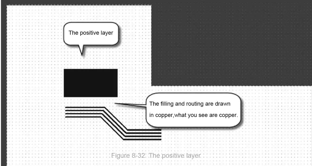
The negative layer is precisely the opposite, and the copper is laid by default. The entire layer has been copper-coated after the negative layer is generated. The routing is the parting line, but no copper exists. The things that should do is spilled the copper laying and set up the copper network after the segmentation. As shown in Figure8-33.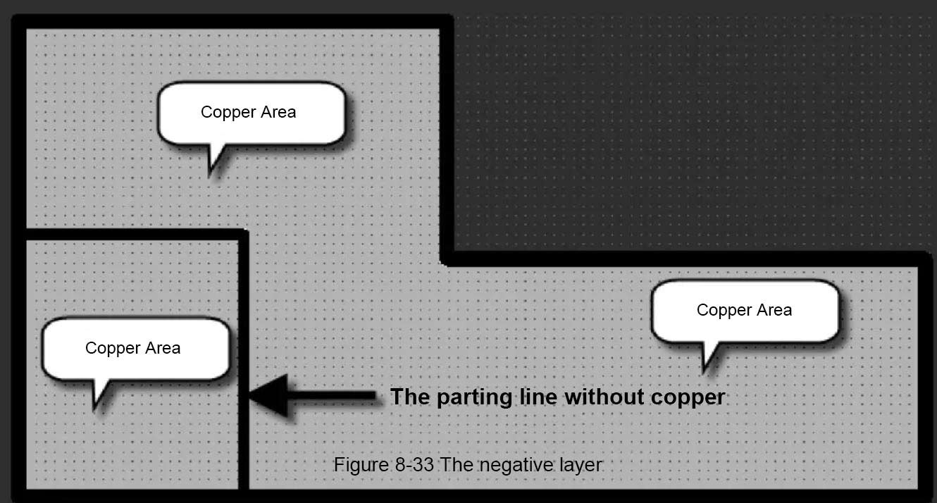
l Realization of internal electrical layer division
In Protel, the internal voltage is split by “splitting,” but the current version of Altium Designer 19 uses “line” or shortcut “PL” to split. The parting line should not be too thin, and you can choose 15mil and above. When splitting the copper laying, draw a closed polygon box with “line” and double-click the copper inside the box to set the network. As shown in Figure8-34.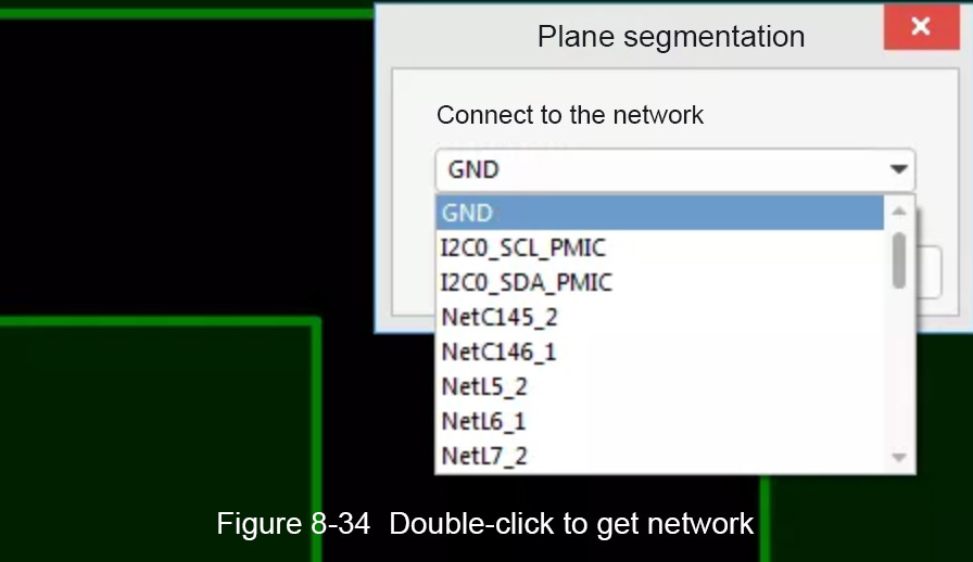
Both the positive and negative layers can be used for the internal electrical layer. The positive layer can also be achieved through routing and copper laying. The advantage of the negative layer is that the default filling of larger copper laying, then the operations of adding through-holes and changing the size of copper laying do not need to re-coat the copper, which will save the time of copper laying calculation. When using the power layer and GND layer (also known as the ground plane) in the middle layer, the layer covers with large copper. Then the advantage of using a negative layer is apparent.
l The understanding of PCB stack-up
With the continuous emergence of high-speed circuits, the PCBs are also getting more complicated. The signal layer and the power layer must be separated to avoid the interference of electrical factors. Then the design of multilayer PCBs is needed. Before designing multilayer PCBs, designers should first determine the PCB structure according to requirements of the circuit size, circuit board size, and electromagnetic compatibility (EMC), that is, to decide whether to use 4-layer, 6-layer, or more-layer circuit boards. This is the simple concept of multilayer PCB designing.
After determining the number of layers, designers need to determine the placement of the internal electrical layers and how to distribute different signals on these layers. This is the point of the stack-up structure of multilayer PCBs. The stack-up structure is a crucial factor influencing the EMC performance of PCBs. An excellent stack-up design will greatly reduce the influence of electromagnetic interference (EMI) and crosstalk.
The layers’ number of the PCB is not the more the better, nor the less the better. There needs to consider many factors to determine the stack-up structure of multilayer PCBs. In terms of routing, the more layers, the better for layout. But the cost and the difficulty of PCB fabrication will also increase. And the symmetry of the stack-up structure is the focus in PCB fabrication for manufacturers. Therefore, designers should consider all aspects to achieve the best balance when determining the layers.
Experienced PCB designers will focus on the problematic points of PCB routing after completing the pre-layout of components, and then determine the number of signal layers based on the quantity and the type of the signal circuit with particular routing demands. Next, the designers will determine the number of layers in the inner electrical layer according to the power types, isolation, and anti-interference requirements.
l Common PCB stack-up
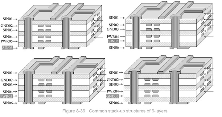
After the number of PCB layers is determined, the next step is to arrange the circuit layers in a reasonable order. The common stack-up structures of 4-layers and 6-layers are listed respectively in the Picture 8-35 and the picture 8-36.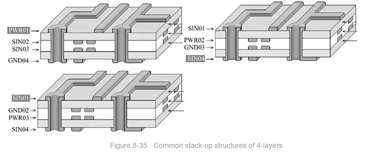
l The analysis of stack-up
How to design the stack-up? Which one is better? Designers usually follow the basic principles as following:
1. The component surface and the welded surface is a complete ground plane (shielding).
2. No adjacent parallel circuit layers as far as possible.
3. All the signal layers are as close to the ground plane as possible
4. The key signal is adjacent to the ground plane and does not cross the segmentation area.
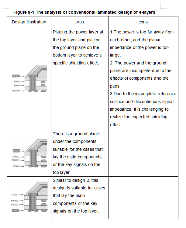
We can analyze the conventional laminated designs shown in figure 8-35 and figure 8-36 according to the above principles.
The analysis indicates as follows:
1. The pros and cons of the three common 4-layers’ laminated designs are shown in figure 8-1.
2. The pros and cons of the four common 6-layers’ laminated designs shown in figure 8-2.
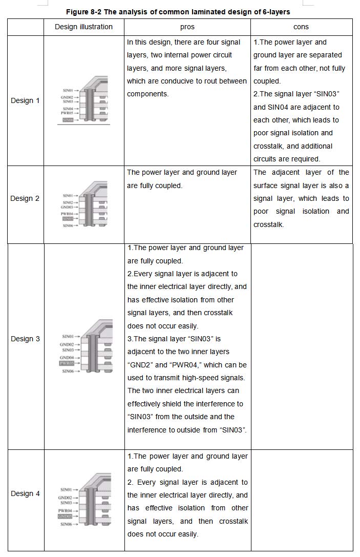
Through the comparison of design 1 to design 4, we can find that design 3 and design 4 are superior to the previous two designs in the case of prioritizing signal priority. But in the actual design, designers usually will choose design 1 to do a stack-up structure considering the cost and layout density. Therefore, designers should pay more attention to the signal cross routing of the two adjacent signal layers and try to minimize crosstalk.
Figure 8-37 shows the recommendation stack-up structure design of the common 8-layer. Design 1 and design 2 are preferred, and design 3 is available.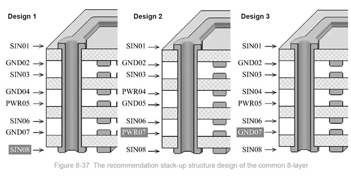
lThe addition and edition of layers
How to add layers in Altium Designer after the stack-up design is determined. Let’s read the following example.
1. Execute the main menu command “design-layer stack manager” or press the shortcut key “DK.” Enter the layer stack manager as shown in Figure 8-38, and set related parameters.
2. Right-click and execute the command of “Insert layer above” or “Insert layer below,” then add a positive layer or negative layer. Running the command of “Move layer up” or “Move layer down” to adjust the order of added layers.
3. Double-click the corresponding name, and you can usually change the name to TOP, GND02, SIN03, SIN04, PWR05, BOTTOM. The name uses the form of “letter +layer number” to read and identify easily. Altium Designer 19 comes with this function.
4. Set the thickness of the laminate layer according to the stack-up structure.
5. Set the inner shrinkage of the negative layer to meet the design of 20H.
6. Click the “OK” button to finish the setting of the stack-up. The stacking effect of a 4-layer board shows in Figure 8-39.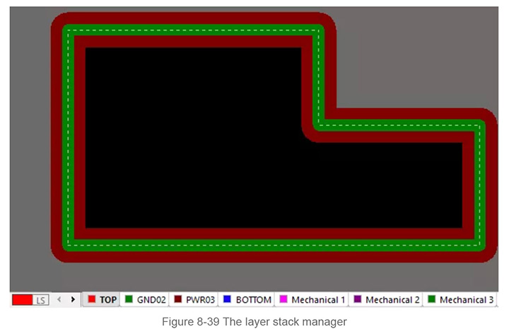
We suggest the signal layer is processed in positive mode, and the power layer and the ground layer are processed in negative mode, which can greatly reduce the amount of file data and improve the design speed.
Still, need help? Contact Us: support@nextpcb.com
Need a PCB or PCBA quote? Quote now
Still, need help? Contact Us: support@nextpcb.com
Need a PCB or PCBA quote? Quote now