
 NextPCB Capabilities
Printed Circuit Boards
NextPCB Capabilities
Printed Circuit Boards
 PCB Assembly
 Layer Buildup
 SMD-Stencils
 PCB Design-Aid & Layout
 Mechanics
 Quality
 Drills & Throughplating
 Factory & Certificate
 PCB Assembly Factory Show
Certificate
PCB Assembly Factory Show
Certificate
Support Team
Feedback:
support@nextpcb.com


A very important advantage of multi-layer boards over ordinary double-layer boards and single-layer boards is that signal lines and power supplies can be distributed on different board layers to improve signal isolation and anti-interference performance. The inner electrical layer is a copper film layer, the copper film is divided into several isolated areas, the copper film in each area is connected to a specific power supply or ground wire through a via hole, thereby simplifying the routing of the power supply and the ground network. At the same time, the internal resistance of the power supply can be effectively reduced.
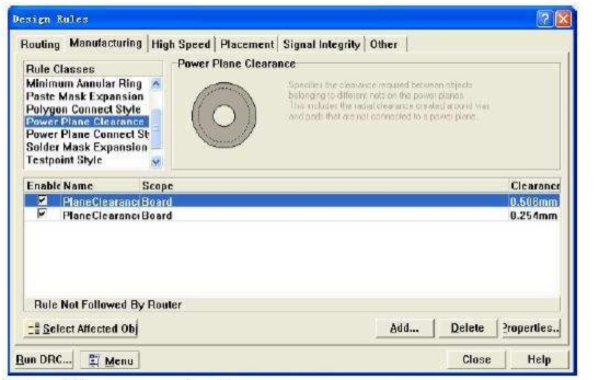
The inner electric layer is usually a whole piece of the copper film, and the pad with the same network name as the copper film will automatically connect it to the copper film when it passes through the inner electric layer. The connection form of the pad/via and the internal electrical layer, as well as the collection of copper film and other pads that are not part of the network, and the safety clearance for common progress can be set in the Power Plane Clearance option. Select the [Design]/[Rules...] command and click the Manufacturing option. The Power Plane Clearance and Power Plane Connect Style options are related to the internal electrical layer. The contents are introduced as follows.
This rule is used to set the safety distance of the inner electric layer, which mainly refers to the safety distance between the pads and vias that are not connected to the inner electric layer and the inner electric layer, as shown in Figure 1. During manufacturing, the pads without a network connection to the inner electric layer will corrode the surrounding copper film when they pass through the inner electric layer, and the size of the corroded ring is the value set in the constraint.
This rule is used to set the form of the pad and the internal electrical layer. Mainly refers to the form when the pads and vias that have a network connection with the inner electric layer are connected to the inner electric layer. As shown in Figure 2.
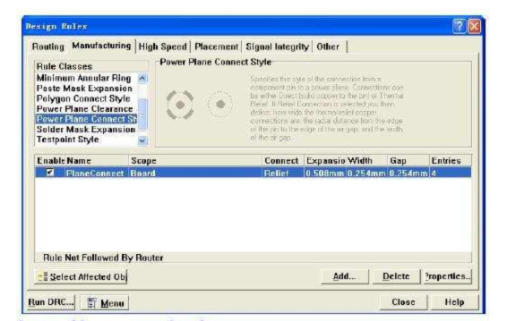
Click the Properties button to pop up its rule-setting dialog box, as shown in Figure 3. The left side of the dialog box is the scope of application of the rule. In the Rule Attributes drop-down list on the right, you can select the connection method: Relief Connect,
Direct Connect and No connect. Direct Connect means direct connection, the pad does not corrode the surrounding copper film when passing through the inner electric layer, and the pad is directly connected to the copper film of the inner electric layer; No connect means no connection, that is, the welding with the same name as the copper film network The disk will not be connected to the internal electrical layer; designers generally use the system’s default Relief Connect connection form, the setting dialog box of this rule is shown in Figure 3.
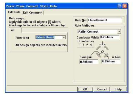
This type of pad connection maintains the connection with the inner electrical layer through conductor expansion and insulation gap. The conductor outlet width is set in the Conductor Width option; the number of conductor outlets is selected in the Conductors option, and you can choose 2 or 4; in the Expansion, option Set the width of the extended part of the conductor; set the width of the insulation gap in the Air Gap option.
In the first few sections of this chapter, we have introduced the selection of the laminated structure of the multilayer board, the establishment of the internal electrical layer, and the related settings. In this section, we will mainly introduce the method and steps of the division of the internal electrical layer of the multilayer board for readers' reference.
2-4 days quick turn prototyping for multi-layer PCB
(1) Before dividing the inner electric layer, you first need to define an inner electric layer. This has been introduced in the previous chapters, so I won't repeat it here. Select the [Design]/[Split Planes...] command, and the internal electrical plane split dialog box shown in Figure 4 will pop up. The Current split planes column in this dialog box refers to the area where the inner electric plane has been split. In this example, the internal electricity, the layers have not been divided, so the Current split planes column shown in Figure 4 is blank. The Add, Edit, and Delete buttons under the Current split planes column are respectively used to add a new power area, edit the selected network and delete the selected network. The Show Selected Split Plane View option below the button is used to set whether to display the schematic diagram of the currently selected split plane of the internal electrical plane. If this option is selected, a thumbnail of the network area divided by the area in the internal electrical layer will be displayed in the box below it, and the pin, pad, or connection with the same name as the internal electrical layer network will be higher in the thumbnail It will be highlighted. If this option is not selected, it will not be highlighted. Show Net For option, select this option. If a network has been assigned to the internal electrical layer when defining the internal electrical layer, the connection and pins with the same name as the network will be displayed in the box above the option.
(2) Click the Add button, and the internal electrical layer segmentation setting dialog box shown in Figure 5 will pop up.
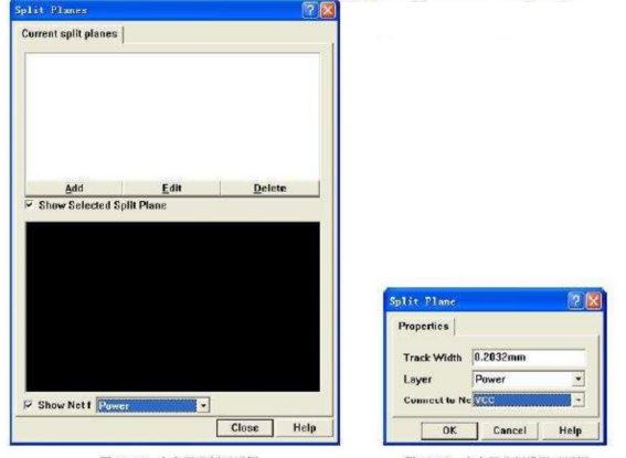
In the dialog box shown in Figure 5, Track Width is used to set the line width when drawing the border, and it is also the insulation distance between different network areas on the same internal electrical layer, so Track Width is usually set to be relatively large. Suggest readers
Also, enter the unit when entering the value. If only numbers are entered here and no units are entered, the system will default to the units in the current PCB editor. The Layer option is used to set the internal electrical layer of the specified division, here you can select the Power and GND internal electrical layers. In this example, there are multiple voltage levels, so it is necessary to divide the Power inner electric layer to provide different levels of voltage for the components.
The Connect to Net option is used to specify the network connected to the divided area. Usually, the inner electric layer is used for the layout of the power and ground network, but as you can see in the Connect to Net drop-down list, you can connect the entire network of the inner layer to the signal network is used for signal transmission, but the general designer does not handle it like this. The signal voltage and current required by the signal are weak, and the wire requirements are small, while the power supply current is large, and a smaller equivalent internal resistance is required. So the general signal is routed on the signal layer, and the inner electrical layer is dedicated to power and ground network connection.
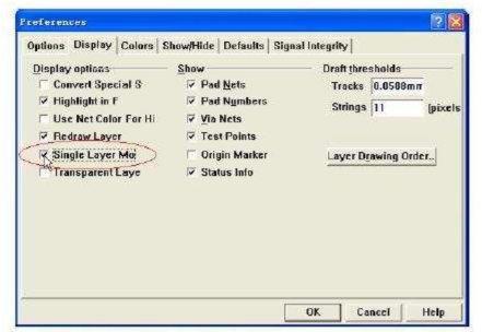
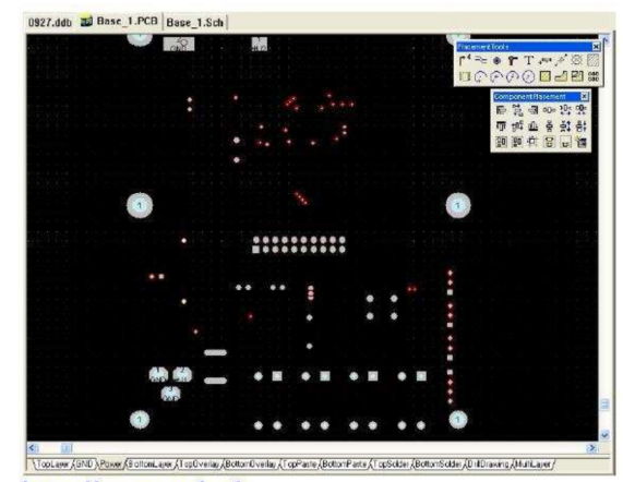
(3) Click the OK button in the electrical layer segmentation setting dialog box in Figure 5 to enter the network area border drawing state. When drawing the inner electrical layer frame, the user generally hides the information of other layers and only displays the currently edited inner electrical layer to facilitate the drawing of the frame. Select the [Tools]/[Preferences...] command, and the dialog box shown in Figure 6 pops up. Select the Display option, and then select the Single Layer Mode check box, as shown in Figure 6. In this way, except for the current working layer Power, the other layers are hidden, and the display effect is shown in Figure 7.
When dividing the inner electric layer, because the divided area includes all the pins and pads of the network, the user usually needs to know the distribution of the pins and pads with the same name as the power network in order to perform the division.
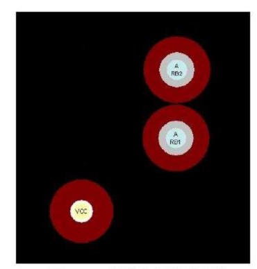
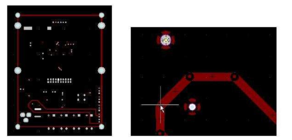
Select the VCC network in the Browse PCB tool on the left, and click the Select button to highlight the network. Figure 8 shows the difference between the pads and pins of the network labeled VCC and other network labels after the VCC network is lit and selected.
After selecting these network pads with the same name, you can include these pads in the divided area when drawing the boundary. At this time, these power supply networks can be connected to the inner electrical layer directly through the pads instead of connecting through the signal layer.
Select [Design]/[Split Planes...] command, the internal electrical plane splitting dialog box shown in Figure 4 pops up, click the Add button, and the internal electrical plane splitting setting dialog box shown in Figure 5 pops up. First, select the 12V network, click OK
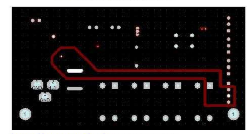
Press the button and the cursor turns into a cross shape, and you can start dividing the internal electrical layer at this time.
When drawing the borderline of the frame, you can press "Shift+Spacebar" to change the corner shape of the trace, or press the Tab key to change the properties of the inner electrical layer. After drawing a closed area (the start point and the endpoint coincide), the system automatically pops up the inner electrical layer segmentation dialog box shown in Figure 9, in which you can see a segmented area, in the PCB editing interface As shown in Figure 10. After adding the internal electrical layer, zoom in on a certain 12V pad, you can see that the pad is not connected to the wire, but a "+" appears on the pad, indicating that the welding disk has been connected to the inner electrical layer. Switch the current working layer to the Power layer, and you can see the connection status of the pad on the internal electrical layer. Since the internal electrical layer is usually a whole piece of the copper film, the part shown around the pad will be corroded during the manufacturing process. It can be seen that the GND and the internal electrical layer are insulated. After adding a 12V area to the internal electrical layer, you can also add other networks according to actual needs, that is, divide the entire Power internal electrical layer into several different isolated areas, and each area is connected to a different power network.
After completing the segmentation of the inner electrical layer, this section will introduce several issues that need to be paid attention to during the segmentation of the inner electrical layer.
Still, need help? Contact Us: support@nextpcb.com
Need a PCB or PCBA quote? Quote now


 Surface

