
 NextPCB Capabilities
Printed Circuit Boards
NextPCB Capabilities
Printed Circuit Boards
 PCB Assembly
 Layer Buildup
 SMD-Stencils
 PCB Design-Aid & Layout
 Mechanics
 Quality
 Drills & Throughplating
 Factory & Certificate
 PCB Assembly Factory Show
Certificate
PCB Assembly Factory Show
Certificate
Support Team
Feedback:
support@nextpcb.com


PCB Artist is a totally free software program device. It is simply among several PCB format software application devices offered to utilize, yet an understanding of one design device can quickly move to any type of PCB layout device. The only constraint is that PCB Artist will certainly not result in a Gerber (. grb) declare basic usage to be produced anywhere, however a.fab data that has to be made with Advanced Circuits. PCB Artist software can be downloaded and install totally free at www.4pcb.com.
When you open PCB Artist for the very first time you will certainly be welcomed with a display like a picture 1 . To open up a brand-new job you can either most likely Submit -> New or push the empty web page switch that is highlighted in the picture 1. The program will certainly that motivate the individual to examine if they desire a brand-new job, a brand-new schematic, or a brand-new PCB format as seen in picture 2. After that pick a location in your documents system to conserve the task on your computer system.
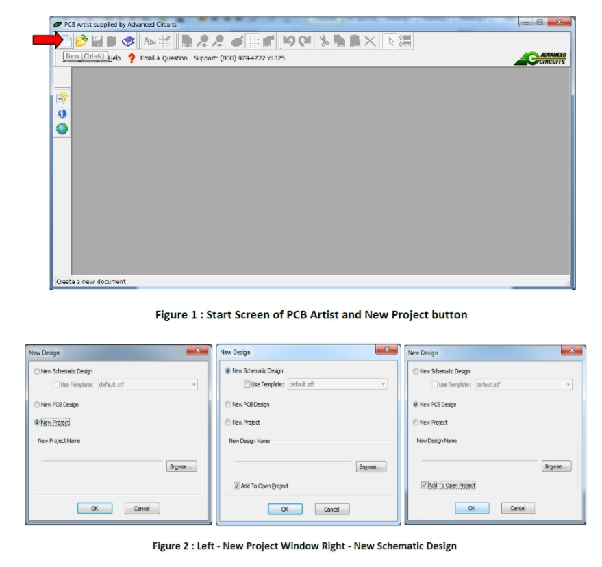
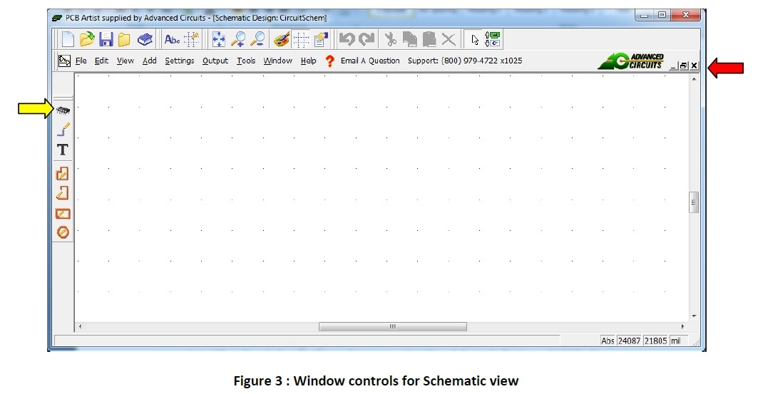
Following developing a brand-new schematic by mosting likely to Submit -> New, or the empty web page switch much like when making a brand-new job. When the home window like picture 2 shows up, choose New Schematic Layout and also Contribute To Open Up Job. Conserve the schematic in the very same folder as the job documents. After conserving the program will certainly open up the schematic sight. The Task, schematic, and also PCB each have their very own sight as well as controls. In the leading right edge of the program highlighted by the red arrowhead in picture3, are the controls for the existing home window you are seeing. You can reduce the home window within the program, optimize it within the program home window, as well as shut it. On the left side of picture 3, the yellow arrowhead explains the device bar that has actually stood for the schematic home window.
The exact same treatment for making a brand-new schematic is exactly how you can additionally develop a brand-new PCB design, yet after developing it there are alternatives you need to establish. A wizard will certainly direct you with the PCB arrangement.
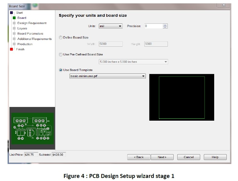
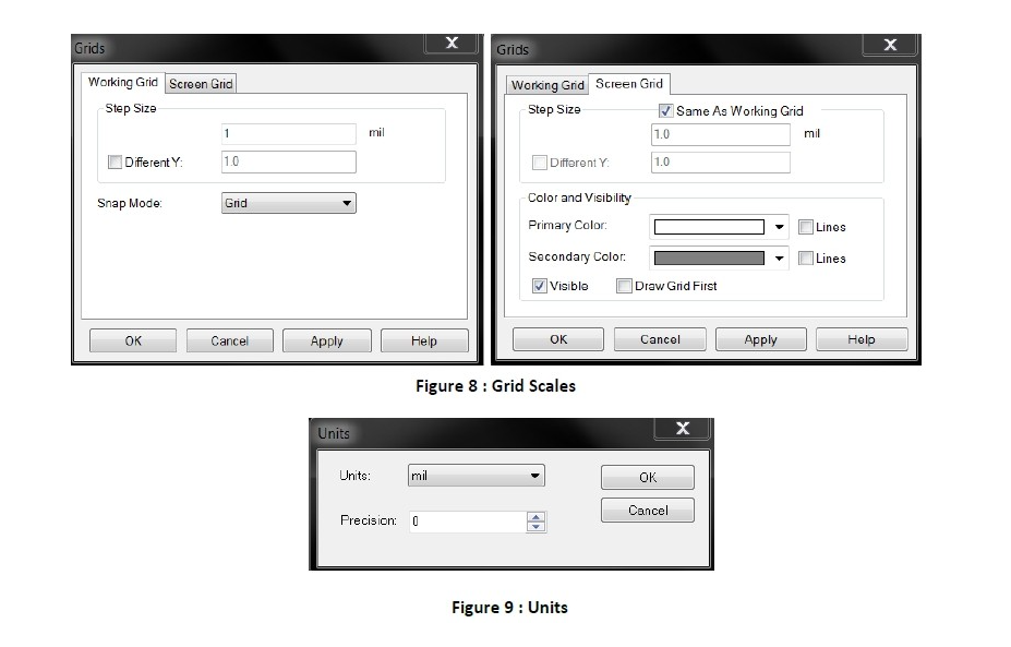
Establish devices to "mils" and also accuracy to "0", mils is 1/1000th of an inch, as well as accuracy, is the variety of locations to the right of the decimal. A value of "1" for accuracy would certainly permit dimensions such as 15.8 mils, yet not 15.75 mils. For 15.75 mils, accuracy must be readied to "2". Usage 'basic minimums for board layout.
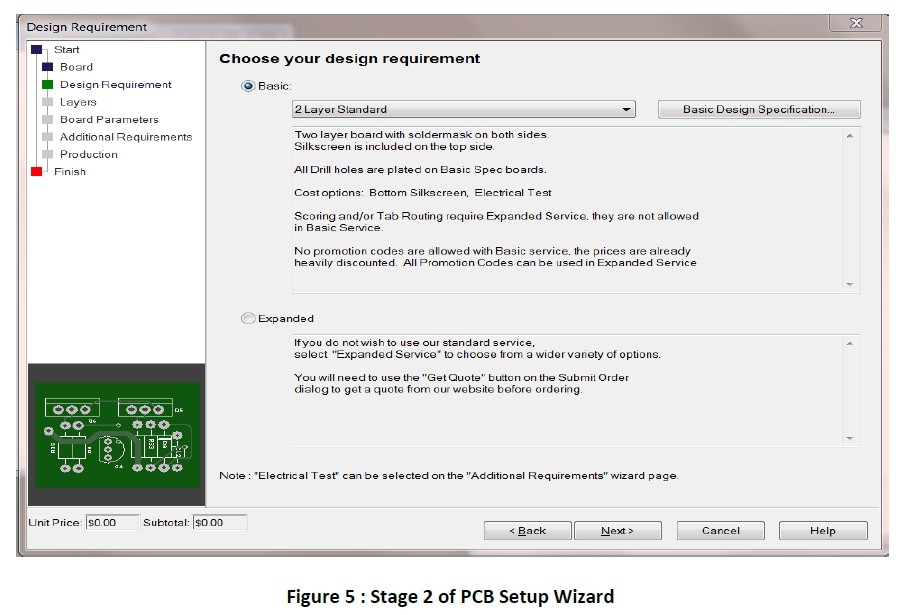
For this basic circuit we will certainly not require greater than 2 layers, so pick the standard choice and also 2 layer requirement.
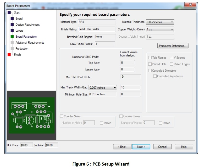
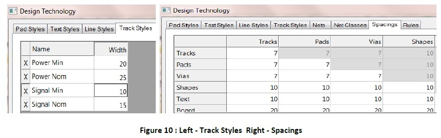
Establish the Minutes. Track Width/Gap to.007 inches as well as leave the remainder at default.
At this stage set the turn-around time to 1 week and also the amount to the wanted quantity. After that call the board as well as the modification. Next off struck coating unless you wish to modify the name of the PCB that you establish previously.
Next off most likely to Setups -> Designs and also match these setups in picture 10.
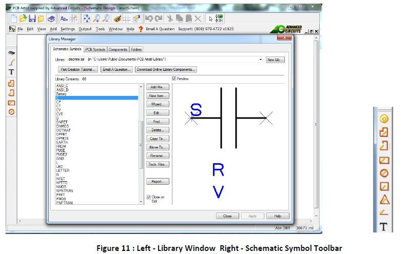
When developing a layout in PCB Artist, elements need to be made use of to develop the circuit in the schematic. These parts will certainly have a schematic icon and also a PCB sign. The part will certainly additionally know connecting just how these 2 signs connect to each other to ensure that the software program can inspect that the schematic and also the PCB design suit. The software application features are constructed in collections of typical components such as resistors, capacitors, adapters, electronic IC's as well as analog IC's, yet there are still lots of components that are not in these constructed in collections. To locate a component to contribute to the schematic, click the switch with a black digital chip on the left side toolbar. In order for this to include in the schematic the schematic home window has to be picked or made best use of in the program. The yellow arrowhead in picture 3 is indicating this switch. If they are not in the collections, after that the component can be produced.
Schematic signs can be produced by either clicking heaven publication in the leading device bar or most likely to Submit -> Collections ..., which additionally has a directory alongside it. To make it very easy to locate the components you made the first thing you ought to do is develop a schematic signs collection. To develop your very own collection click the New Lib switch in the leading right edge of the Libraries home window as well as get in the name of your collection and also wait. This will certainly open up the home window seen in picture 4, to reach the schematic icons choose the schematic signs tab. By clicking the New Thing ... a brand-new home window will certainly open up. In this home window, a brand-new schematic icon can be developed by attracting forms as well as lines utilizing the brand-new toolbar on the left side of the home window displayed in Picture 4. The leading switch in picture 4 is the Include Pad switch, a Pad is where the schematic sign will certainly have the ability to be linked-to in the schematic with various other components, additionally can be called a pin.
To show exactly how to make a schematic icon an instance of making a 7404 6 inverter electronic IC will certainly be shown. This IC has 14 pins as well as can be any type of dimension in the schematic, as long as it has actually all the needed links. ICs can be conveniently made via the schematic icon wizard, by defining the quantity of pins as well as alignment in the wizard, the program can attract the sign for you. The wizard switch is simply listed below the New Thing ... switch in the Schematic Sign tab. Picture 6-9 reveals the go through of the wizard.
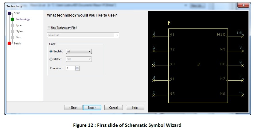
For the initial slide, displayed in picture 5, make certain the systems are English as well as mil is picked. This indicates this schematic sign will certainly be gauged in thousandths of an inch.
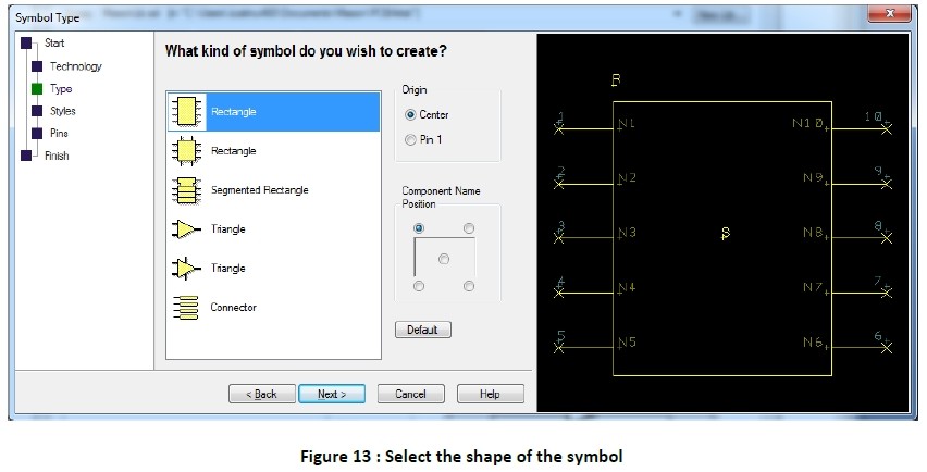
The kind phase of the wizard permits you to pick various forms for usage in producing a schematic sign. For this IC the rectangle form will certainly be made use of.
This phase defines the number and also positioning of pins. The pins do not need to be balanced as well as can be picked to spiral around the IC, or number from leading down on both sides. This can be made to match the real IC pin numbers however matching the performance is what is very important when mapping pins, not what they are phoned number. That being claimed, matching the numbering of the pins to the real IC can be useful.
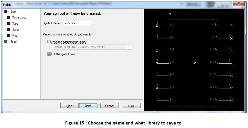
This phase enables you to call the sign, as well as which collection it will certainly be conserved. You can likewise pick the choice to modify the sign currently to include in the icon. To make it less complicated to check out the sign and also recognize the IC a lot more will certainly be contributed to the icon.
As displayed in picture 9, with use the illustration devices a much more detailed icon can be made. After ending up making alterations, conserve the sign by clicking the Save switch, or most likely to Submit -> Conserve as well as select the collection you produced previously.
An element can just be made use of if it has both a schematic sign as well as a PCB Sign. As a result if you might not locate the part you require in the typical collections and also have actually made a customized schematic icon you can affix that schematic icon to an existing PCB Icon or develop your very own. For direction on just how to connect existing PCB icons, dive to the Linking Schematic and also PCB Symbols area. If you are mosting likely to be producing your very own PCB sign the wizard for the PCB Symbols is much more efficient than the Schematic Icon Wizard. First develop a brand-new part collection by clicking heaven publication or Documents -> Collections to open up the Libraries home window. Select the PCB Symbols tab and after that click the New Lib ... switch, this will certainly open up a home window to call and also conserve your collection. To begin the wizard, click the Wizard switch while on the PCB Symbols tab.
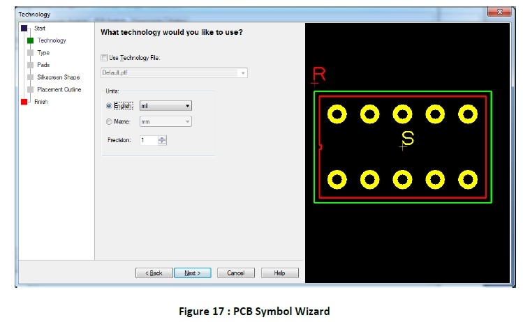
This wizard begins comparable to the schematic wizard; the setups for this web page need to coincide.
To figure out what impact you intend to pick you have to examine the information sheet of the component you are producing to discover the readily available bundles and after that select which you will certainly purchase. "DIP" as well as "AXIAL" are impacts that are additionally called via opening because the pins will certainly copulate via the board. Others like "SOIC", "QFN", "SOT", as well as "BGA" remain in a group called surface area install due to the fact that they just link outside layer pads.
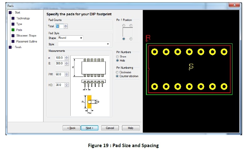
This phase permits you to select the pad dimension as well as spacing. Suit these measurements with the datasheet of the chip; ensure you are taking a look at the appropriate bundle on the datasheet. For the Silkscreen Forming phase as well as the Positioning rundown phases leave the setups at default unless you particularly wish to alter these setups, which will just boost the silkscreen of the impact. The silkscreen is the message and also forms that will certainly be published in white ink on the board to aid determine the positioning of components on the PCB.
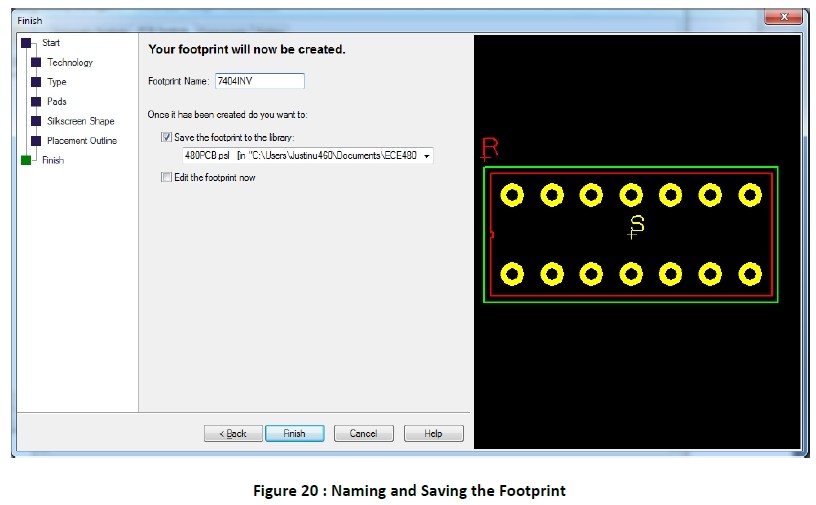
The last of the PCB symbol wizard permits you to call the impact and also select what collection the impact will certainly be conserved in.
To complete developing a part a schematic sign have to be connected to a PCB icon to ensure that the software application can associate the pins in between both. Most likely to the collections home window by clicking heaven publication on the leading toolbar or mosting likely to Submit -> Collections. After that most likely to the Parts tab as well as click New Lib ... to after that call and also conserve your elements collection. Alongside begin producing a part click the New Thing ... switch under the Parts tab, this will certainly open the home window in Picture 21.
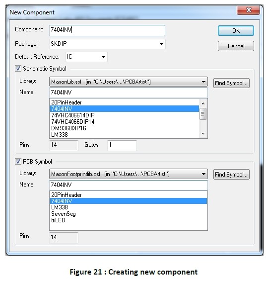
Enter in the wanted name of the element the bundle kind and also a Default Referral that will certainly turn up on the schematic and also PCB unless transformed to one more name or erased. The bundle name and also Default Referral are not crucial yet should be completed. After that pick the schematic collection which holds your wanted schematic and also pick the schematic. After that do the exact same for the PCB icon. Next off struck he OKAY switch.
KEEP IN MIND: Any kind of schematic or PCB signs can be utilized in producing a part; you can make use of a custom-made schematic sign you produced with a PCB sign that was currently in one more collection or vise versa.
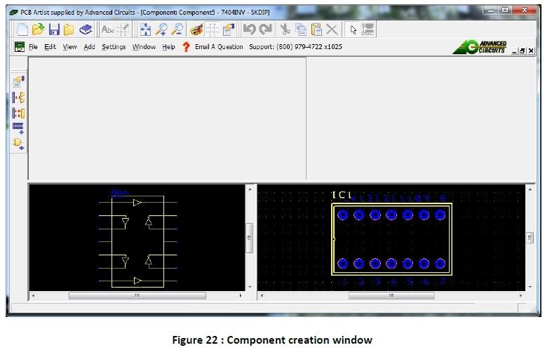
Picture 22 is what you need to see after striking the OKAY switch from picture 21. To obtain table in picture 23 appropriate click in the vacant gray area over the schematic as well as PCB signs.
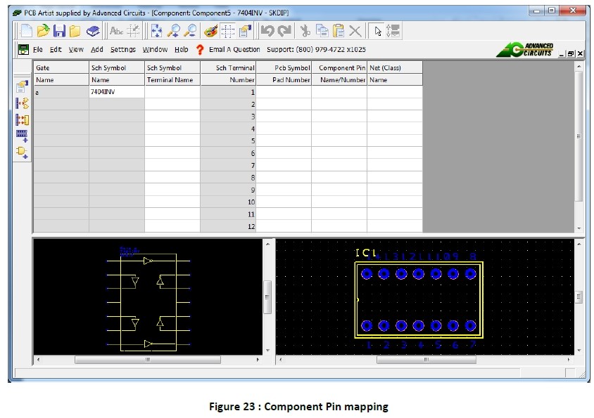
Currently, fill out the PCB Sign Pad picture column to match the Schematic Terminal picture to the appropriate pins. It must resemble picture 24 when you finished this. You can include names to the Terminals as I finished with the Vcc and also GND pins.
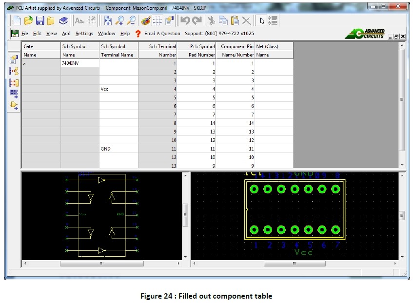
Complete the element by clicking the Save switch or mosting likely to Submit -> Conserve to conserve the element. You can select to modify the name or collection it will certainly be conserved in after that struck OK. You must currently see the part you made in the collection you picked to wait in.
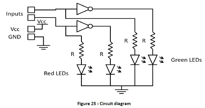
Schematic design is the academic side of the PCB. It defines exactly how the circuits will certainly function by revealing the links from pin to pin. The PCB we will certainly develop in this tutorial will certainly regulate 4 LEDs with 2 input signals. There will certainly be 2 eco-friendly LEDs and also 2 red LEDs, when the input signals are high the red LEDs will certainly get on and also when the input signals are reduced the eco-friendly LEDs will certainly get on. Picture 25 is a layout of what the schematic ought to be.
To begin we will certainly include the 7404 IC we developed previously in this tutorial. Open up the schematic home window otherwise currently open. You can do this by dual clicking the schematic name in the job home window. Following click the Include Element switch, after that choose the collection that holds the part you desire to contribute to the schematic. After that undergo the collection to discover the component.
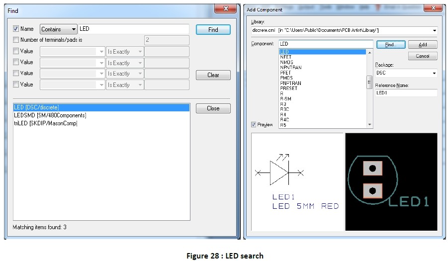
KEEP IN MIND: The Locate ... switch can be made use of to look for elements in all collections by the name, part of the name, variety of terminal/pins, as well as much more.
When you have actually discovered the element you intend to include click the Include switch, this will certainly affix the schematic sign to your computer mouse to be put where you click. Currently we require to locate adapters for GND VCC and also the input pins. Most likely to the adapter collection and also locate the 4WP part. picture27 is what the part needs to appear like.
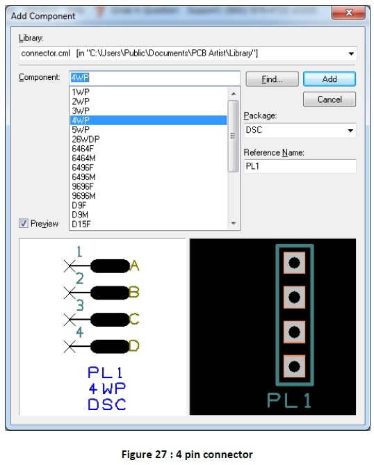
Include this adapter to your schematic by clicking the Include switch. Next we will certainly include the LEDs, click the Discover ... switch to open up a look for parts. Fill in the search like it remains in Picture 28. When you pick among the search results page the sneak peek will certainly appear in the Include Part home window, see to it the LED is via opening, you can inform this by openings in grey pads as opposed to strong rectangular shapes. The proper LED is revealed on the best side of Picture 28.
After including 4 LEDs we should currently include the resistors. Most likely to the collection called resistor and also explore the collection till you discover a via opening resistor and also the bundle is R 0.500. These are current restricting resistors and also there is one for every LED so location 4 of them in the schematic.
KEEP IN MIND: When selecting parts like capacitors as well as resistors, if the PCB footprint coincides with the value of the resistor in the schematic will certainly not matter.
KEEP IN MIND: To turn the picked element simply struck the "r" secret to revolve in a counter-clockwise movement.
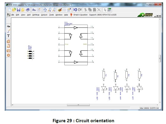
Orient your schematic to make sure that it looks like the circuit layout over. It ought to resemble picture 29 listed below.
KEEP IN MIND: You can get rid of the lengthy names from parts by dual clicking the name and also un-checking Recommendation Call from the Program location of the alternatives.
To begin circuitry these parts with each other either dual click the x at one of the terminals (pins) of any kind of element or click the Include Schematic Link switch and afterwards click the incurable you intend to the cable to begin with. After that click the incurable you intend to attach the various other end of the cable to. Make the links according to the circuit layout.
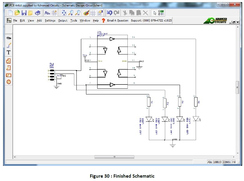
Currently include the GND as well as VCC elements to stay clear of going across cords. This can be done by including the GND and also VCC parts from the schema collection. Considering that the physical positioning is not established by the schematic specific signs like GND or VCC can be made use of to work as a solitary node in the schematic. In the PCB format nevertheless the links will certainly need to be all literally made with each other. picture30 is what your schematic ought to resemble.
Conserve the schematic by clicking the Save switch or most likely to Submit- > Conserve.
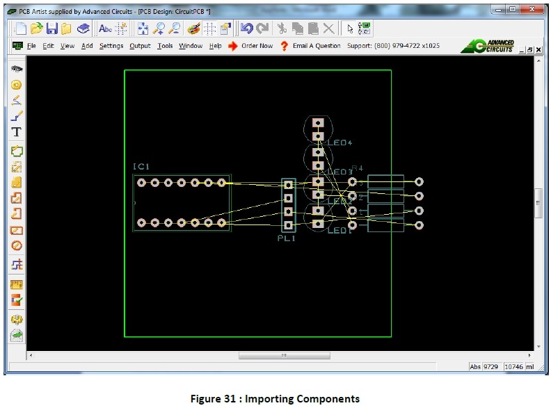
Open up the PCB design home window by dual clicking the PCB layout name in the job home window. To import the elements from the schematic most likely to Devices -> Schematic<-->PCB -> Uniformity Examine, this will certainly open up a Note pad home window with the distinctions as well as a verification home window asking if you desire the program to make the modifications. Click Yes to import the elements that remain in the schematic. After that struck OKAY on the following verification that appears. Leave out of the Notepads as well as zoom out in the PCB style home window. In the bottom left edge you will certainly see the impacts of the elements that remain in your schematic. The yellow lines are links that remain in your schematic informing you where you require to make links in the PCB.
Relocate and also revolve the parts around till the least quantity of yellow lines are crossing each other. We can do this given that in the circuit we do not mind in what order or where the LEDs are since this has to do with finding out exactly how to make use of PCB Artist not the circuit itself. There are various means to orient the PCB picture 32 reveals one means.
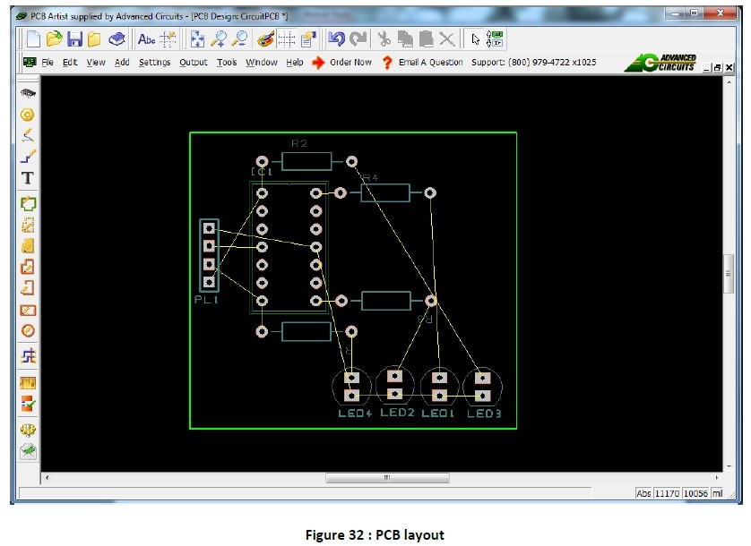
You can change the dimension of the board by clicking as well as dragging the eco-friendly lines. Turning parts and also tags likewise functions similarly as in the schematic design. To start circuitry click the Include Track switch and afterwards click a pad similar to in the schematic format.
KEEP IN MIND: After clikcing a pad, the ideal hitting -> Sector Setting -> Miter, will certainly make your traces straight lines with 45 level angles. This is suggested since 45 level transforms look even more specialist that appropriate angles.
With the continuing to be links we have a couple of choices, we might most likely to the 2nd layer to go under various other traces or we can walk around and also under the resistors. The yellow line from the GND pin to the GND side of the LEDs is simply that, a ground link. When making a PCB devoting a layer to GND is constantly a great concept to lower sound and also various other issues with the circuit. Running a trace via the 2nd layer is not needed for this circuit however, for the benefit of understanding I will certainly go through an instance.
To run a trace under an additional trace you can include a by means of to the PCB as well as link the trace to it, after that run a trace on the 2nd layer past the trace in the means. After that include an additional by means of to bring the trace back to the leading layer to attach to the pad. This can be done by including a trace from the initial pad to an open location in the board hitting when to establish the range of the trace and afterwards best clicking -> Following Layer.
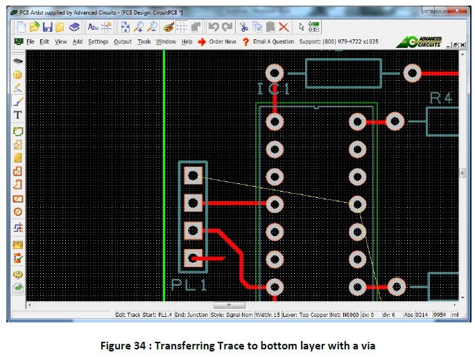
This will instantly include a by means of and also alter the trace layer to the 2nd layer (all-time low layer for this PCB). After that attract the trace past the traces initially in the method as well as repeat the actions that made the very first using yet pick previous layer as opposed to following layer. This will certainly bring the trace back to the leading layer to make sure that you can attach to pad. The 2nd by means of is needed for a component that would certainly be surface area placed, yet because our parts are with opening the bottom layer trace can link straight to the with opening pad.
KEEP IN MIND: Given that the 2nd layer for our PCB will certainly be devoted to the Ground aircraft making links via the 2nd layer will certainly interfere with the connection of the ground airplane which serves however the larger the interruption the even more sound and also various other troubles might develop in the circuit, so maintain these 2nd layer traces as well as brief as feasible.
KEEP IN MIND: To eliminate yellow lines of a link that has actually been made go to Equipment -> Enhance Internet.
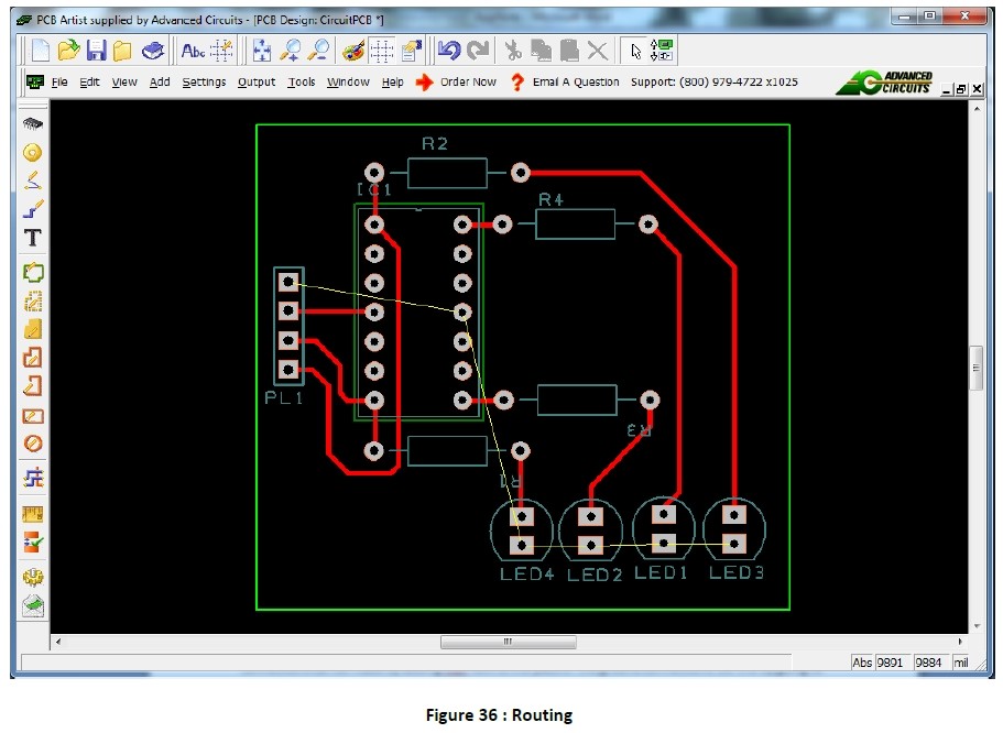
Picture 36 reveals the transmitting without making use of the 2nd layer. Considering that the 2nd layer will certainly be ground, all links can be made by including vias alongside the pads of the ground links. Do this by mosting likely to Include -> Via, put the by means of near the pad to be attached to ground. This is displayed in Picture 37.
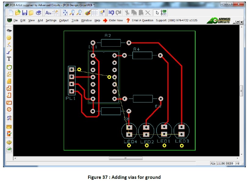
After that link these vias with traces to the pads. Given that we have actually not put the ground layer it will certainly ask if you intend to combine GND with the web of the by means of, click yes. Next we will certainly attract package to "pour copper" to develop a ground aircraft under layer. To attract a box for a copper put click the Include Location for Copper Pour switch. After that attract a box throughout the whole board as received picture 38. Ensure the layer it is attracting is the 2nd layer, as well as when you have a box press go into to complete it.
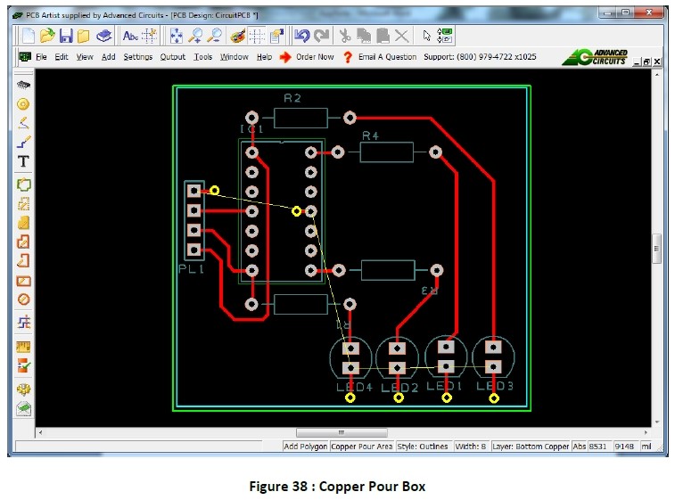
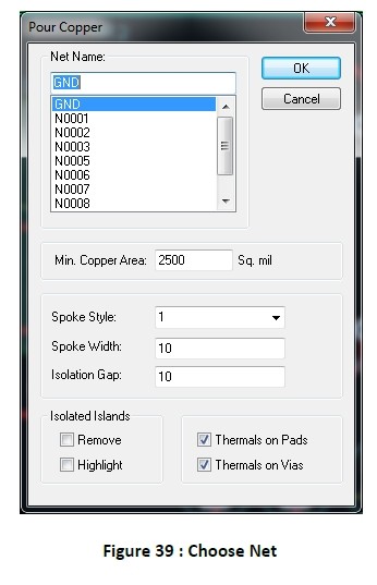
Select among the lines of the copper put box, ideal click -> Pour Copper. This will certainly raise the home window in picture 39 to pick what web to connect to the copper, select GND as well as click OK.
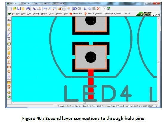
Currently the copper will certainly be loaded. If you zoom out and also focus the graphics will certainly freshen and also you will certainly after that have the ability to see your elements on the board. If you focus on the links to ground you can see that there are bridges to the with opening links like in picture 40. This reveals that the vias alongside these pads are not required given that the program understood that the via opening elements can be linked to on the 2nd layer. If these were surface area place parts the vias would certainly be required. Because they are not required I will certainly eliminate them and also clear after that put the copper once more to fill out the holes left by the vias.
We currently have actually a finished PCD layout, to include tags or messages to the silkscreen, make use of the Include Text switch.
Still, need help? Contact Us: support@nextpcb.com
Need a PCB or PCBA quote? Quote now


 Surface

