
 NextPCB Capabilities
Printed Circuit Boards
NextPCB Capabilities
Printed Circuit Boards
 PCB Assembly
 Layer Buildup
 SMD-Stencils
 PCB Design-Aid & Layout
 Mechanics
 Quality
 Drills & Throughplating
 Factory & Certificate
 PCB Assembly Factory Show
Certificate
PCB Assembly Factory Show
Certificate
Support Team
Feedback:
support@nextpcb.com


1. According to the layout principle of "big before small, difficult before easy", that is, important unit circuits and core components should be given priority.
big before small, difficult before easy
2. The layout should refer to the principle block diagram and arrange the main components according to the main signal flow direction of the single board. The layout shall meet the following requirements as far as possible: the total connection line shall be as short as possible, and the key signal line shall be the shortest; The layout of the decoupling capacitor should be close to the power pin of the IC as far as possible, and the circuit between the decoupling capacitor and the power supply and the ground should be the shortest; Reduce the wrong way of the signal running and prevent accidents on the road.
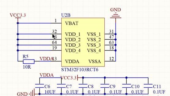
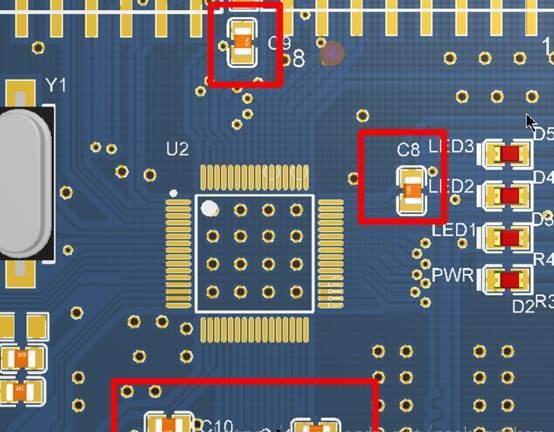
For example, in the figure below, C8 to C11 are decoupling capacitors between VCC and GND. There is no way to reflect their position requirements in the schematic diagram. However, the PCB should be placed in the input pin accessories of the chip power supply. For example, there should be capacitance near the 31 and 32 pins, and there should be capacitance near the 18 and 19 pins.
The correct example is close to the power input pin of the chip
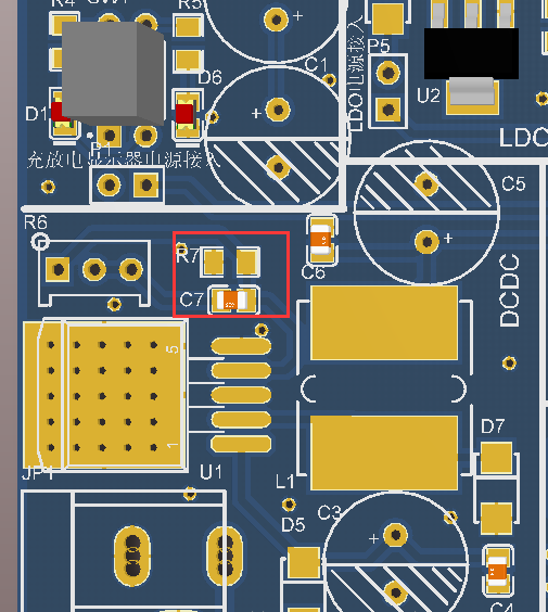
3. The arrangement of components should be convenient for debugging and maintenance, that is, large components cannot be placed around small components, and there should be enough space around the components to be debugged, which often makes the situation very embarrassing. As shown in the following figure, R7 and C7 are difficult to be welded if the surrounding devices are welded first( It also shows that the welding sequence is very important.)
4. For the same circuit structure, the "symmetrical" standard layout should be adopted as far as possible; The layout is optimized according to the standard of uniform distribution, the balanced center of gravity, and a beautiful layout.
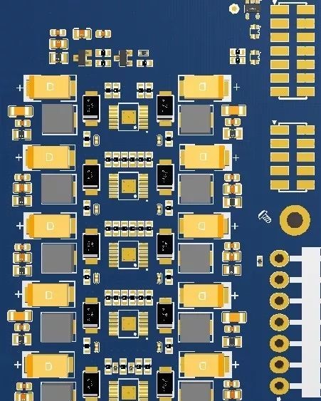
5. The same type of plug-in components should be placed in one direction in X or Y direction. For the same type of polarized discrete components, it is also necessary to strive to keep consistent in the X or Y direction, to facilitate production and inspection( If the polarity of the device needs to be confirmed manually, the production cost may rise.)
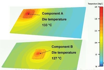
6. The heating elements should be evenly distributed to facilitate the heat dissipation of the single board and the whole machine, and the temperature-sensitive elements other than the temperature detection elements should be far away from the components with large heat. In addition to temperature sensors, triodes are also heat-sensitive devices.
7. The signals of high voltage and high current are completely separated from the weak signals of low current and low voltage; The analog signal is separated from the digital signal; The high-frequency signal is separated from the low-frequency signal; the High-frequency components should be fully spaced. In the layout of components, it should be considered that the components using the same power supply should be put together as far as possible to facilitate the separation of power supply in the future.
The above is about "how to put" that is, the main considerations of the layout. On the other hand, how to connect is more complicated
Priority of key signal line: simulate key signals such as small-signal, high-speed signal, a clock signal, and synchronous signal;
The principle of density priority: start from the device with the most complex connection relationship on the single board. Starting from the most densely connected area on the board.
The self-service guide of wiring can be summarized as follows:
If the layout is not appropriate, the board may be very inconvenient to use, and the wiring is very difficult.
When layout, the devices that complete a certain function should be close to each other as much as possible. There are some operation skills. Next, give an example.
You can first find the device of the op-amp module in the schematic diagram, press and hold Ctrl to select. In the PCB, these devices have also been selected.
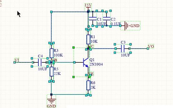
Then observe the connection relationship in the schematic diagram, for example, C4 is connected to R3, R5, Q1. Find these devices in PCB and put them together.
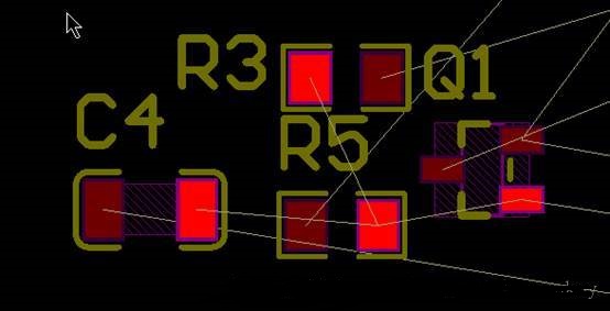
Observe the pre pull wire situation. It is known that each device has a common network called VB. You can press Ctrl to select a pad with VB attribute selected, then VB will highlight.
After the device is imported into PCB, the layout shall be completed according to the requirements.
Then there are signal lines, whether serial port, 485 or can, signal line should be as short as possible, less through the hole, sometimes also match length, such as difference. In addition, sometimes clock line, such as crystal vibration, also need to be short, with less drilling through the hole.
Still, need help? Contact Us: support@nextpcb.com
Need a PCB or PCBA quote? Quote now


 Surface

