
 Surface


Stacy Lu

 NextPCB Capabilities
Printed Circuit Boards
NextPCB Capabilities
Printed Circuit Boards
 PCB Assembly
 Layer Buildup
 SMD-Stencils
 PCB Design-Aid & Layout
 Mechanics
 Quality
 Drills & Throughplating
 Factory & Certificate
 PCB Assembly Factory Show
Certificate
PCB Assembly Factory Show
Certificate
Support Team
Feedback:
support@nextpcb.com


Contents
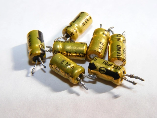
Electrolytic Capacitors (E-caps) are a specialized type of capacitor, fundamentally different from common ceramic capacitors (non-polarized) due to their construction and polarity. The anode of an electrolytic capacitor uses a “valve metal” such as tantalum or aluminum. An oxide layer forms on the surface of the metal through electrolytic treatment in an appropriate solution, and this layer acts as the dielectric (insulator). It is the rectifying characteristic of this oxide layer that imparts intrinsic polarity to the electrolytic capacitor.
Therefore, as a PCB designer, you must strictly adhere to the polarity requirements. Electrolytic capacitors should be considered as having zero tolerance for reverse voltage; some aluminum electrolytics may tolerate a minute reverse bias of ≤ 1 V under specific conditions, but manufacturers often specify 0 V or impose stringent limitations (time and temperature restricted). The official datasheet must be the definitive standard. Depending on the cathode material, electrolytic capacitors are broadly categorized into those using a liquid electrolyte (wet type) and those using conductive polymers (solid type). This structural difference directly impacts their electrical performance, lifespan, and PCB layout requirements.
> Recommend reading: The Footprint Files: Electrolytic Capacitors

Accurate selection of electrolytic capacitors is the foundation for subsequent PCB layout optimization. Designers must look beyond nominal capacitance and gain a deep understanding of parasitic effects and environmental dependencies.
The actual performance of an electrolytic capacitor is determined by its Equivalent Series Resistance (ESR), Equivalent Series Inductance (ESL), and nominal capacitance (C). ESR is the core parameter determining a capacitor’s transient response capability and thermal performance. In power applications, a low ESR value is crucial because it effectively minimizes power loss (P = Irms2 × ESR) and heat generated by the ripple current flowing through the capacitor. Excessive ESR not only increases ripple voltage but also causes the capacitor temperature to rise, accelerating its aging.
ESL is primarily determined by the capacitor’s internal winding structure and lead length. ESL, along with the capacitance value, determines the capacitor’s Self-Resonant Frequency (SRF, fR = 1 / (2π √(L C))). Most aluminum electrolytics have an SRF in the tens of kHz to several hundreds of kHz, while smaller volume or polymer series can push this up to several hundreds of kHz to a few MHz. Therefore, in the frequency band > several hundred kHz to MHz, decoupling is predominantly handled by MLCCs or low-ESL devices.
Ripple current is the main cause of internal heating and accelerated aging in electrolytic capacitors, especially in switching power supply applications. Designers must first convert the peak-to-peak ripple voltage (Vpp) into RMS ripple current (Irms). The Irms value must be determined based on the waveform and impedance: If the voltage spectrum across the capacitor is known, Irms = Vrms / |Z(ω)|, where Z must include both ESR and capacitive reactance; if the loop current is known, the Irms of the capacitor branch current is used directly. The primary design requirement is to ensure the actual RMS ripple current is kept below the manufacturer’s specified rated capacity to guarantee thermal stability and reliability. Practical design relies on the “rated ripple current” limit given in the datasheet as a hard constraint, combined with subsequent temperature rise evaluation. Furthermore, implementing voltage derating is standard practice for enhancing long-term reliability.
Retrieved from:
The expected lifetime of liquid aluminum electrolytic capacitors is highly correlated with their internal temperature. Electrolyte evaporation follows the Arrhenius equation, meaning lifetime strictly depends on temperature. The widely accepted “10°C rule” states that the service life approximately doubles for every 10°C reduction in the capacitor’s internal temperature. Thus, a capacitor rated for 5,000 hours at 105°C can be expected to have a service life of 20,000 hours at 85°C. PCB designers must use effective thermal management and derating to keep the actual operating temperature well below the rated maximum to meet the system’s required long-term service life.
In complex power network design, using the standard series R-L-C model to predict the impedance characteristics of aluminum electrolytic capacitors is often insufficient. The physical structure of an aluminum electrolytic capacitor is complex, behaving as a lossy coaxial distributed RC circuit element. This means its capacitance (C), ESR, and impedance vary significantly with changes in frequency and temperature.
Of particular note is the temperature dependence of ESR. The mobility of ions in the electrolyte is influenced by viscosity, and ESR decreases significantly with increasing temperature, typically ranging from tens of percentage points to several-fold improvement, with the magnitude strongly dependent on the model and frequency. While a drop of 40% to 80% may occur when the temperature increases from 25°C to 85°C, designers must always rely on the ESR-vs-Temperature/Frequency curve provided in the datasheet.
Without using complex SPICE models that incorporate frequency and temperature dependence in PDN impedance analysis, simulations will fail to accurately reflect the circuit’s performance at high and low temperatures. This temperature-dependent ESR behavior creates a design paradox: while reducing temperature prolongs lifespan, excessively low operating temperatures (e.g., during cold start) can increase ESR, potentially pushing the PDN impedance peak beyond the Target Impedance Mask, thereby compromising system stability. Thus, thermal design must be a trade-off that balances lifespan and electrical performance.
Electrolytic capacitors are primarily used to provide bulk capacitance. For this bulk storage function to be effective, large-value capacitors (typically 10 μF to 100 μF) must be placed as close as possible to the power pins of the load IC. The general rule of thumb suggests these capacitors should be placed no more than 2 inches (approx. 50 mm) away from the IC. This rule is a rough heuristic for bulky storage/electrolytic capacitors and is acceptable for low-frequency/input-side storage.
For high-switching-current applications, such as DC-DC converters or motor drivers, layout stringency is much higher. For high-speed/high di/dt loops (like near switching nodes or core power outputs), the distance must be far less than 2 inches. The design must adhere to the principle of “loop area as small as possible,” achieved through planes and multiple vias for low ESL implementation. The high di/dt loops in these circuits (including input capacitors, switching elements, and output capacitors) must be designed to be as narrow and compact as possible. A smaller loop area results in lower parasitic inductance (L), thus minimizing transient voltage spikes (Vspike = L × di/dt). As switching frequency and current slew rates increase, even the low-frequency storage loop of electrolytic capacitors must approach the standards of high-frequency MLCCs, meaning the actual distance should be far less than 2 inches to strictly control the parasitic inductance budget.
Power integrity relies on providing a low-impedance return path. PCB designers should ensure that the power and ground planes are continuous and adjacent. Placing decoupling capacitors close to the IC’s power and ground pins minimizes the current path to the power and ground planes. The key to adjacent power and ground planes is close coupling (adjacent layers V/GND forming a low-inductance return path); “symmetry” is not a mandatory requirement, but continuity and proximity to the return vias are more critical. Designers should also minimize the number of layers between the planes and the capacitor connections, which helps reduce loop inductance and improve PDN performance.
Since the lifespan of liquid electrolytic capacitors is highly sensitive to temperature, PCB layout must prioritize temperature control. First, avoid clustering heat-generating components (like power transistors, rectifiers, etc.) to prevent localized hotspots, ensuring proper heat dissipation and thereby improving component reliability. Second, active cooling measures should be taken for the capacitor itself or its nearby heat sources. For example, placing heat-sensitive components near heatsinks or using thermal vias to enhance heat conduction and dissipation. Effective thermal management is the only way to utilize the 10°C rule to extend the capacitor’s service life.
The quality of the routing connection to the electrolytic capacitor directly determines whether its low-ESR/low-ESL performance can be effectively realized. Even a large capacitance value is limited by the parasitic inductance of the traces and vias in the connection path.
> Recommend reading: The Ultimate PCB Routing Guidelines
When designing power input and high di/dt loops, traces must be designed to be short and wide to minimize resistance and inductance. In high-current and high-power circuits, designers must consider the target current, the maximum allowable temperature rise, copper foil thickness, and trace resistance. To increase current carrying capacity and minimize voltage drop, designers should consider using thicker copper layers (e.g., 2 oz or higher) or exposing copper and adding solder to increase trace thickness. Simultaneously, solid copper pours should be used in high-current paths for power planes to distribute current evenly and further reduce resistance.
PCB designers must follow a clear current connection sequence to ensure the capacitor is on the shortest decoupling path. Best practice recommends that when connecting to a power plane via vias, the connection should first go from the component pin to the capacitor pad, and then to the via and the power plane. This connection logic ensures continuous current flow through the capacitor on the decoupling path, optimizing noise filtering. In high-current applications, vias need to be placed strategically, and their current carrying capacity must be calculated. Using multiple vias to connect the power plane and capacitor pads (e.g., using “stitching vias” in multi-layer boards) helps to distribute current evenly and reduce local impedance.
> Recommend reading: PCB Prototyping Basics: DFM, Stackups, Impedance, HDI, Files & Cost
For Surface Mount Device (SMD) electrolytic capacitors, pad design is not just the basis for electrical connection but also affects mechanical reliability. Oversized pads can lead to the formation of excessively large solder fillets during soldering, which can transfer undue thermal or mechanical stress to the capacitor body or dielectric. Mechanical stress sensitivity is particularly high in tantalum capacitor applications. Pad design should reference industry standards, with a recommendation to use newer land pattern specifications like IPC-7351 (A/B), and prioritize the manufacturer’s recommended land pattern. In applications with extreme vibration, adhesives may also be needed to pre-fix components, reducing the likelihood of failure induced by mechanical stress.
Table 2: Electrolytic Capacitor PCB Layout and Routing Key Checklist
| Design Element | Design Principle | Implementation Detail |
|---|---|---|
| Decoupling Distance | Transient Current Response Optimization | 10 μF – 100 μF electrolytics placed ≤ 50 mm (2 in) from the IC (bulk/low-frequency). Closer for high di/dt nodes. |
| High di/dt Loop | Minimize Current Loop Area (L) | Place near IC power/ground pins; short, compact paths; use adjacent power/ground planes. |
| Connection Sequence | Minimize Path Impedance | Current path: component pin → capacitor pad → via. |
| High-Current Traces | Minimize Resistance (R) | Use wide, short, thick copper; multiple stitching vias to planes. |
| Safety Clearance | Prevent Secondary Failure and Explosion | Keep-out above the safety vent per datasheet (e.g., φ18–35 mm → ≥ 3 mm). |
| Thermal Management | Extend Service Life | Keep away from heat sources; add thermal vias or copper pours near the capacitor. |
The primary failure mode for liquid aluminum electrolytic capacitors is electrolyte evaporation, which leads to reduced capacitance and dielectric strength. To prevent explosion from excessive internal pressure caused by overvoltage, high ripple current, or reverse voltage, aluminum electrolytic capacitors are typically equipped with a safety vent to release internal gases.
However, improper manufacturing handling (such as degradation from cleaning solvents) or low barometric pressure environments (like airborne applications) can cause the safety vent to open prematurely or unintentionally, leading to electrolyte evaporation and corrosive leakage.
For low-pressure environments, capacitors of the appropriate rating (aerospace/automotive/industrial grade) must be selected and evaluated according to the manufacturer’s altitude/pressure specifications. Low pressure changes the external pressure on the case and the electrolyte evaporation rate, which can indeed reduce margin, but a blanket prohibition is not appropriate; rely on qualified devices and validation.
Safety vent layout is a critical element of PCB safety design. Designers must ensure that the area above or around the pressure relief vent has absolutely no circuit patterns, traces, or components. The required clearance distance depends on the case diameter (empirical guide; always defer to the series datasheet):
When mounting on double-sided PCBs, prohibit traces or components directly above/below the vent and avoid obstructing airflow. The capacitor body should not sit over any circuit patterns or unused vias.
Once venting occurs, the released electrolyte is corrosive and can damage PCB copper traces and surrounding components. The reserved clearance serves to isolate the venting area both vertically and horizontally, preventing secondary failures and system-level damage.
Certain high-performance or high-density capacitors, such as wet tantalum capacitors, are extremely sensitive to environmental stress and mechanical vibration. High vibration can cause anode connection wire fracture (open circuit) or abrasion of the tantalum pellet, leading to electrolyte contamination and a significant rise in ESR. Mounting orientation and mechanical fixation (e.g., adhesives) are therefore critical.
An ideal power network would have zero impedance. The practical design goal is to flatten the impedance curve and keep it as low as possible by paralleling multiple capacitors. The principle of multistage decoupling utilizes differences in SRF to cover a wide frequency span. Electrolytic capacitors, due to large capacitance and higher ESR, mainly cover the low-frequency band (DC to several hundred kHz) for energy storage. MLCCs, with extremely low ESR/ESL, cover the high-frequency band (MHz to GHz). Note that modern MLCC values are commonly available up to 10–100 μF at lower voltage ratings, but DC-bias derating reduces effective capacitance and must be accounted for.
Table 3: Mixed Capacitor Collaborative Design Strategy — PDN Impedance Matching
| Capacitor Type | Frequency Range | Primary Function | PDN Optimization Goal |
|---|---|---|---|
| Electrolytic Cap (C ≥ 10 μF) | Low (DC–100 kHz) | Energy storage, ripple suppression | Meet low-frequency impedance target; provide low-frequency damping |
| Polymer/Tantalum (C ≈ 1–10 μF) | Mid (100 kHz–10 MHz) | Bridge impedance valley; filter switching noise | Use moderate ESR to suppress anti-resonance peaks |
| Ceramic (MLCC) | High (>10 MHz) | Transient decoupling; HF noise suppression | Lowest possible ESL; keep HF impedance below target |
Anti-resonance Strategy
| Focus | Design Goal |
|---|---|
| Resonant frequency points | Spread SRFs so peaks don’t overlap |
| Damping resonant peaks | Leverage electrolytic ESR or add series R to lower Q |
On the PDN impedance curve, different capacitors form multiple “U”-shaped regions. Electrolytics handle the low-frequency region; after their SRF, impedance rises sharply and MLCCs take over at higher frequencies to suppress noise with very low impedance.
Parallel combinations of capacitors with different L and C can create anti-resonance peaks (high impedance) at certain frequencies, causing significant rail ripple and potential signal integrity issues. Diagnose by frequency sweeping (instrument or simulation) and verify against the target impedance mask.

Electrolytic ESR is a natural low-frequency damper. Polymer and tantalum parts (ESR lower than wet aluminum but higher than MLCCs) serve as bridging components. Spread SRFs, include realistic ESR in SPICE, and where appropriate add series resistors to flatten the impedance curve.
Solid polymer capacitors use conductive polymer electrolytes, yielding extremely low ESR and (package-dependent) low ESL. This enables high ripple-current handling and reduced temperature dependence compared to wet aluminum types, significantly extending service life. ESL depends on package/leads/layout; SMD polymer parts are generally lower ESL than leaded aluminum electrolytics, but not necessarily lower than small MLCCs.
> Recommend reading: PCB Capacitors: Why Is It Important and How to Choose?
Tantalum capacitors offer very high capacitance density for space-constrained designs. However, solid tantalum is sensitive to reverse bias and surge currents, with a risk of short-circuit and even combustion. Strict derating and surge limiting are required. Polymer tantalum can greatly reduce thermal-runaway risk but still requires derating and surge control.
| Characteristic | Wet Aluminum Electrolytic | Solid Polymer Aluminum Electrolytic | Solid Tantalum |
|---|---|---|---|
| Capacitance Density | High (cost-driven) | Medium-High (performance-driven) | Extremely High (volume-driven) |
| ESR / ESL | Relatively high ESR / medium-high ESL | Extremely low ESR / low ESL | Low ESR / medium ESL |
| Frequency Response | Low-frequency filtering (< 1 MHz) | Excellent; good high-frequency performance | Good; mid-to-high-frequency decoupling |
| Reliability | Lifetime strongly temperature-dependent | Long life; low temperature dependence | No wear-out mechanism; sensitive to surges/mechanical stress |
| Failure Mode | Venting/gas release; evaporation → open/high ESR | Open or high ESR | Short (catastrophic, flammable) |
| Layout Consideration | Strict keep-out for safety vent | Compact volume; lower thermal pressure | Mechanically sensitive; strict derating and fixation |
For solid-state capacitors (polymer and tantalum), designers must elevate mechanical integrity to the same importance as electrical performance. Wet tantalum capacitors are particularly sensitive to vibration and bending; control pad geometry and consider adhesives for fixation. In low-pressure environments, select appropriately rated parts and validate against the manufacturer’s altitude/pressure specifications.
Retrieved from: https://www.researchgate.net/publication/367763135_Electrolytic_capacitor_Properties_and_operation
Electrolytics often sit at power I/O to handle high RMS ripple currents. To minimize heat and drop from ESR-related losses, use wider/thicker copper and robust planes. NextPCB supports heavy copper manufacturing to reduce trace resistance and improve current capacity, directly supporting low-impedance, low-thermal interconnects and improving overall reliability.
PDN optimization depends on controlled stackups and tolerances. Manufacturing support includes material/lamination optimization and impedance verification (e.g., 50 Ω targets), enabling confidence in simulations and ensuring collaborative damping across the band.
With extensive manufacturing experience, early DFM checks mitigate risks from tolerances or design-to-manufacturing mismatches that could degrade electrolytic reliability or PDN performance.
Electrolytic capacitors are primarily used for energy storage, voltage smoothing, filtering, decoupling, and reducing power supply ripple. They help maintain stable voltage levels and improve the overall performance of electronic circuits.
Electrolytic capacitors offer relatively high capacitance values in a compact package, making them effective for filtering voltage fluctuations and smoothing rectified DC output in power supply applications.
Electrolytic capacitors should generally be placed as close as possible to power input stages, voltage regulators, or high-current components that require filtering. Proper placement helps reduce noise, improve power integrity, and minimize unwanted voltage ripple.
Most electrolytic capacitors are polarized components. Reversing the polarity can cause excessive leakage current, overheating, reduced performance, or even capacitor failure. PCB designers and assemblers should carefully verify polarity markings during design and assembly.
The lifespan of electrolytic capacitors is influenced by operating temperature, voltage stress, ripple current, environmental conditions, and component quality. Lower operating temperatures and proper circuit design can significantly extend capacitor service life.

References:
[1] Leite, A. V. T., Teixeira, H. J. A., Cardoso, A. J. M., & Araújo, R. M. E. (2007, June). A simple ESR identification methodology for electrolytic capacitors condition monitoring. In 20th International Congress on Condition Monitoring and Diagnostic Engineering Management (pp. 95–103). Faro, Portugal. Retrieved from https://www.researchgate.net/publication/229017336_A_simple_ESR_identification_methodology_for_Electrolytic_Capacitors_conditon_monitoring
[2] Replace Author(s). (2023). Electrolytic capacitor: Properties and operation. ResearchGate. https://www.researchgate.net/publication/367763135_Electrolytic_capacitor_Properties_and_operation
Still, need help? Contact Us: support@nextpcb.com
Need a PCB or PCBA quote? Quote now

