
 Surface


Arya Li, Project Manager at NextPCB.com

 NextPCB Capabilities
Printed Circuit Boards
NextPCB Capabilities
Printed Circuit Boards
 PCB Assembly
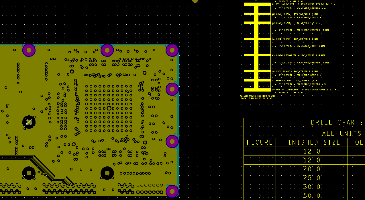
 Layer Buildup
 SMD-Stencils
 PCB Design-Aid & Layout
 Mechanics
 Quality
 Drills & Throughplating
 Factory & Certificate
 PCB Assembly Factory Show
Certificate
PCB Assembly Factory Show
Certificate
Support Team
Feedback:
support@nextpcb.com


Introduction
When working on a complex PCB layout, designers tend to rely heavily on the DRC (Design Rule Check) engine within their CAD software to spot errors that could reduce manufacturing yield. However, reliance on DRC alone is not always sufficient. Some electrically correct design choices will create DFM (Design for Manufacturing) problems that need to be identified and rectified before sending a PCB out for manufacturing.
PCB designers typically perform these checks in their layout file before it is exported to Gerber files, but the Gerber files themselves should always be reviewed independently before a board is sent to the fabrication house.
The list of design and DFM problems below is not exhaustive, but these are critical areas that any designer should verify before releasing their data to a manufacturer. There are 6 common DFM problems found in many PCB designs:
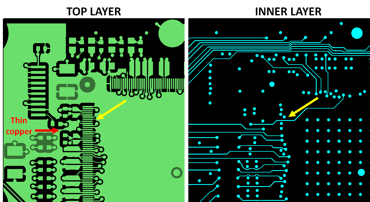
In the example above, thin copper can be identified in the top layer, and there may be a clearance problem between traces and vias on the inner layer.
It is important to note that these design problems might not trigger an electrical DRC error unless you have specifically configured complex design rules for these DFM points in your PCB design software. Therefore, designers need to check their Gerber files for these DFM problems either manually or, preferably, with automated Gerber file checker software.
Designers need to review these potential issues before starting their fab run. However, not all designers have access to the enterprise-level CAM engineering software used by professional manufacturers. This usually leaves designers relying on the native DRC engine in their CAD tools or manually scrolling through layers in a basic viewer. Here are the risks associated with manual checks:
With so many potential risks before fabrication, PCB designers need an automated solution to ensure efficiency and accuracy.
The fastest way to spot manufacturability problems in your Gerber files is to use dedicated software. Most applications accept Gerber files in RS-274X and X2 formats, while others support IPC-2581, ODB++, or native CAD files.
These applications are designed to simulate the manufacturing process and spot problems that will reduce fabrication or assembly yield. The best Gerber checking programs provide specific benefits beyond simple viewing:
Example: CAD tools often apply 1 mil clearances by mistake when grounding a net to a plane or polygon. These vias are supposed to be connected to the surrounding plane, and this clearance mistake can be instantly flagged by an automated checker.
With these capabilities, you can identify design problems before the data reaches the factory floor. Unless you utilize a turnkey service with enhanced inspection, a budget fabricator might not pause production to warn you of these errors, leading to a failed run (scrap).
Ensure your files are error-free and get an instant quote.
No download, no sign-up required for basic viewing, no obligation.
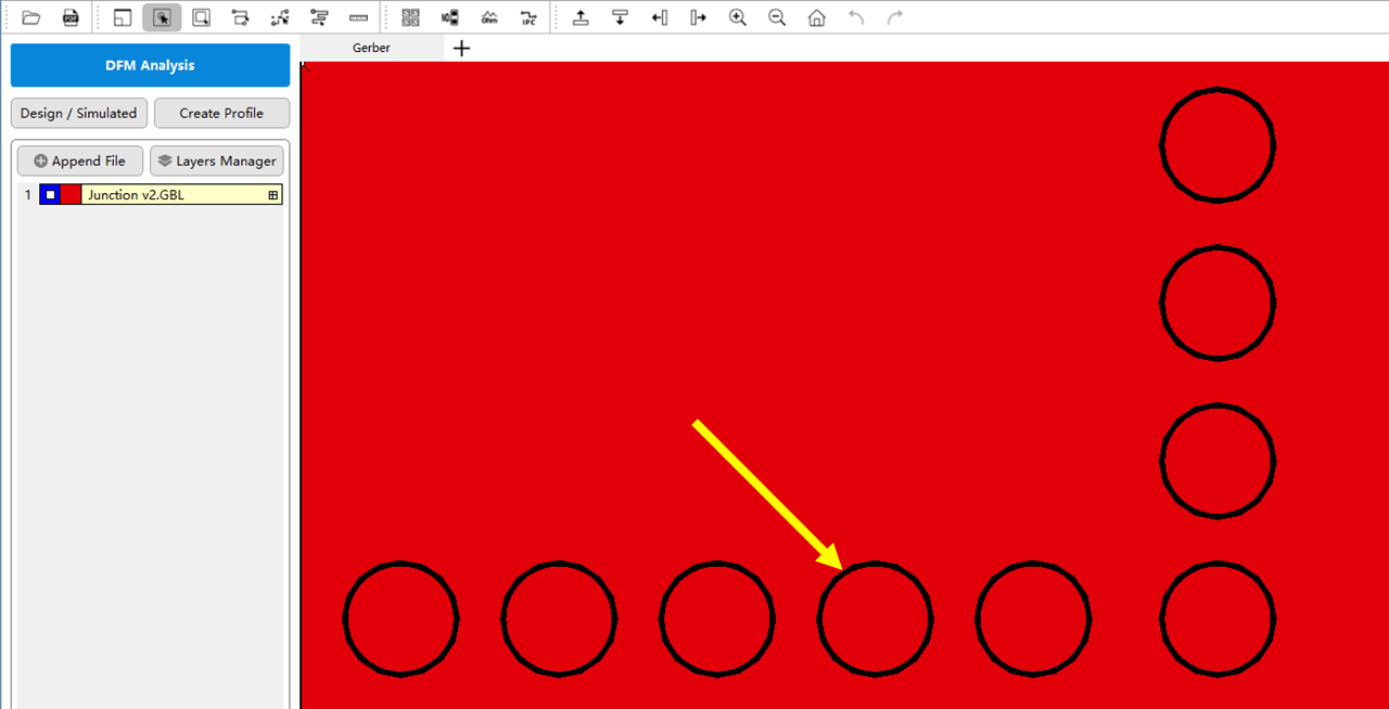
NextPCB Online Gerber Viewer is a free, advanced PCB visualizer with in-depth Design for Manufacture (DFM) analysis capabilities. It supports RS-274x and Extended (X2) Gerber files from a broad range of PCB CAD software, including Altium Designer, OrCad/Allegro, Eagle, KiCad, DipTrace, DesignSpark, and EasyEDA.
Developed by HQ Electronics, HQDFM leverages over 15 years of industry expertise to provide advanced manufacturing insights directly in your web browser.
>> Try Best Free Online Gerber Viewer
Once you have checked your PCB layout in HQDFM, you can seamlessly transition your design into fabrication with NextPCB, one of China’s most experienced and reliable PCB manufacturers. The pricing analysis provided by HQDFM is accurate, ensuring your design passes NextPCB’s engineering review process smoothly.
DRC (Design Rule Check) is performed within your CAD software to ensure the layout meets specific electrical constraints (like trace width and spacing) defined by the designer. DFM (Design for Manufacturing) analyzes the design to ensure it can actually be built by the factory equipment. DFM checks for issues like acid traps, solder mask slivers, and drill aspect ratios that DRC often misses.
Yes, Gerber files can be edited using CAM software (Computer-Aided Manufacturing) or advanced Gerber editors. However, it is generally recommended to make changes in the original CAD source files and re-export the Gerbers to ensure data consistency between your schematic and the final layout.
If your vias are covered, it usually means the "tented vias" option was selected during Gerber generation, or the solder mask expansion was set to zero or a negative value. If you need exposed vias for testing, ensure your solder mask expansion is set correctly in your CAD tool.
For full turnkey PCB assembly, you typically need to provide:
The most reliable method is to use a dedicated DFM tool like the HQDFM Viewer. This software simulates the manufacturing process and highlights areas that violate standard production capabilities, preventing costly delays.

Still, need help? Contact Us: support@nextpcb.com
Need a PCB or PCBA quote? Quote now

