
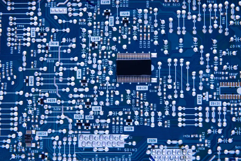
 NextPCB Capabilities
Printed Circuit Boards
NextPCB Capabilities
Printed Circuit Boards
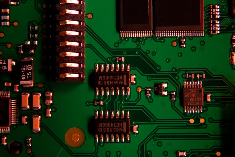
 PCB Assembly
 Layer Buildup
 SMD-Stencils
 PCB Design-Aid & Layout
 Mechanics
 Quality
 Drills & Throughplating
 Factory & Certificate
 PCB Assembly Factory Show
Certificate
PCB Assembly Factory Show
Certificate
Support Team
Feedback:
support@nextpcb.com


Introduction
Every groundbreaking circuit starts somewhere, usually on a small, imperfect prototype. PCB prototyping isn't just a step in the design process; it's the sandbox where ideas are tested, refined, and brought to life. For engineers and technology decision makers, this is the stage where theory meets practice: signal paths are validated, components are stress-tested, and design concepts evolve through iteration.
Whether you're an experienced hardware engineer experimenting with high-speed circuits or a student building your first multi-layer PCB, prototyping allows you to experiment boldly without fear of failure. Mistakes aren't setbacks; they're lessons that reveal how your design behaves in the real world, from thermal performance to signal integrity.
But a playground is only as safe and productive as the tools and partners you choose. A reliable PCB prototyping service, like NextPCB, ensures that your prototypes are fabricated quickly, accurately, and with high-quality materials, letting you focus on innovation rather than manufacturing headaches.
In short, the journey from idea to working prototype is where creativity and engineering meet, and the right support can make that journey faster, smoother, and far more rewarding. This article explores the technical aspects of PCB prototyping, including common challenges engineers face and effective strategies to overcome them. It highlights best practices, modern tools, and materials that enhance the prototyping process.
Prototyping is where design assumptions are tested against reality, and reality often pushes back. Engineers and students alike face recurring technical challenges during PCB prototyping that can determine whether a design fails, functions, or excels. Understanding these challenges is the first step toward building better circuits.
These challenges highlight why prototyping is indispensable, as it exposes weaknesses in a design before it scales into costly production.
The good news is that every prototyping challenge has a modern solution. Today's engineers and students have access to advanced tools, smarter design strategies, and rapid fabrication services that enable the creation of functional prototypes faster and more reliably than ever.
1. Simulation and Pre-Layout Analysis: Simulation tools have become indispensable in modern PCB design. They allow engineers to validate signal integrity, thermal behavior, and power delivery before a single board is fabricated. By catching issues early, simulation reduces wasted iterations and shortens time-to-market. A report shows that digitally transformed PCB companies report a 20% faster time to market, a 15% reduction in defect rates, and a 53% decrease in lead times after adopting digital automation and simulation tools. While most fabricators accept simulation-ready files, many do not yet provide integrated simulation feedback loops. PCB manufacturers could add value by offering pre-fabrication simulation support or direct integration with popular EDA tools, helping customers validate manufacturability and performance side by side.
2. Design-for-Manufacturing (DFM) Checks: DFM is one of the most powerful practices in PCB prototyping. It ensures that the design is manufacturable from the start, catching errors like spacing violations, unsupported drill sizes, or poorly placed vias before they become expensive mistakes. This not only saves money but also improves yield. Optimizing designs with DFM can improve PCB yield from 25% to 88%, reduce production costs by 10–25%, and increase overall manufacturing yield to 98–99% versus the typical 85–90% in non-optimized designs. Many manufacturers provide free DFM checks, but they're often limited to rule violations. PCB companies could go further by offering predictive DFM analytics, showing designers how changes would impact yield, cost, and reliability, transforming DFM from a reactive filter into a proactive design partner.
3. Rapid Fabrication Cycles: Speed matters in prototyping. The faster engineers can get a board in hand, the more iterations they can test and refine. Modern rapid fabrication allows teams to compress design cycles, enabling experimentation and innovation at a much faster pace than traditional methods. Traditional PCB prototyping could take 4–6 weeks, but rapid fabrication services now deliver in 1–5 days, while 3D printing approaches cut this down to 24–48 hours. This shift lets teams prototype multiple times per week instead of waiting months. Fast turnaround is becoming the norm, but PCB companies can differentiate by pairing speed with real-time progress tracking and iteration-friendly pricing models. This would allow engineers—especially students and startups—to affordably test more design variations in less time.
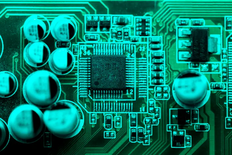
4. Advanced Materials and Processes: Materials and manufacturing processes have a huge impact on prototype performance. High-Tg laminates, low-loss dielectrics, and controlled impedance stack-ups make high-speed, high-density designs possible. For power and RF boards, the right material choice is the difference between failure and reliability. Using high-Tg substrates improves thermal reliability by up to 40%, while controlled dielectric laminates can reduce signal loss by up to 30% in high-frequency applications. Many prototyping services only offer basic FR-4. To truly support innovation, manufacturers could expand accessible material options (e.g., Rogers, polyimide flex, metal-core boards) and provide clear performance data to guide engineers in making informed choices.
5. Documentation and Collaboration: Even the best designs fail without clean documentation. Accurate Gerber files, BOMs, and assembly drawings prevent costly delays and rework. When communication is seamless, fabrication partners can execute more reliably, and engineers spend less time troubleshooting misunderstandings. Poor documentation is behind up to 70% of production delays, according to industry audits. Early manufacturer involvement and organized file submission dramatically reduce re-spins and accelerate time-to-market. Too often, file checks happen late in the process. PCB providers could add value by offering interactive documentation review portals, where engineers and manufacturers co-verify files before production begins, turning documentation from a bottleneck into a collaboration tool.
Together, these practices shorten the path between design and working hardware, empowering engineers and students to focus on innovation rather than troubleshooting preventable errors.
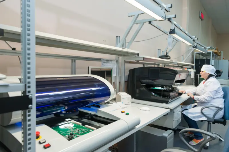
Overcoming prototyping challenges requires not just design discipline, but also a fabrication partner that can keep up with the pace of innovation. NextPCB has positioned itself as one of those partners, delivering speed, precision, and flexibility that support engineers at every stage of prototyping.
1. Fast Turnaround, Multiple Iterations: Where traditional prototyping often took weeks, NextPCB offers rapid fabrication cycles as short as 24 hours for standard boards. This empowers engineers and students to iterate quickly, turning design improvements into working boards without waiting months.
2. Integrated DFM and File Checking: NextPCB provides free, automated DFM reviews that catch common manufacturability issues before fabrication begins. By integrating these checks early, engineers reduce the risk of re-spins and costly delays, and can trust that their design intent will be preserved.
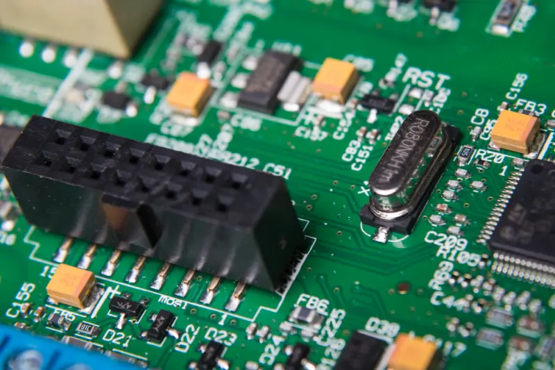
3. Support for Advanced Materials and Technologies: Beyond standard FR-4, NextPCB supports a variety of high-performance laminates, multi-layer stack-ups, HDI, and flex PCB options. This flexibility allows engineers to test cutting-edge designs, whether they're working on high-frequency RF circuits, compact wearables, or power-dense systems.
> Get Advanced PCB Materials at NextPCB
4. Precision Manufacturing and Quality Control: NextPCB operates with tolerances that meet IPC Class 2 and Class 3 standards, ensuring prototypes are not only fast but also reliable enough for rigorous testing. For high-speed and high-density designs, this level of precision is critical in ensuring meaningful prototype validation.
5. Accessible to Students, Startups, and Professionals: Affordability and scalability matter. NextPCB's pricing structure makes it feasible for students and hobbyists to experiment, while still offering the technical depth and capacity required by startups and professional engineers, bringing products closer to mass production.
> Get precision-engineered PCB prototypes in as fast as 24 hours, backed by ISO-certified quality and competitive pricing.
Prototyping is as much about mindset as it is about technical execution. Whether you're a student soldering your first circuit or an engineer fine-tuning a multi-layer design, these practical steps can help you get more value out of every prototype.
1. Start Simple, Scale Gradually: Begin with simpler single-layer or two-layer designs before tackling complex stack-ups. This builds confidence and gives you early wins before moving into high-density layouts.
2. Design with Testing in Mind: Think about how you'll measure performance before you fabricate. Add test points, leave access to critical nodes, and plan for probing during assembly. Prototypes that are easier to test yield better insights.
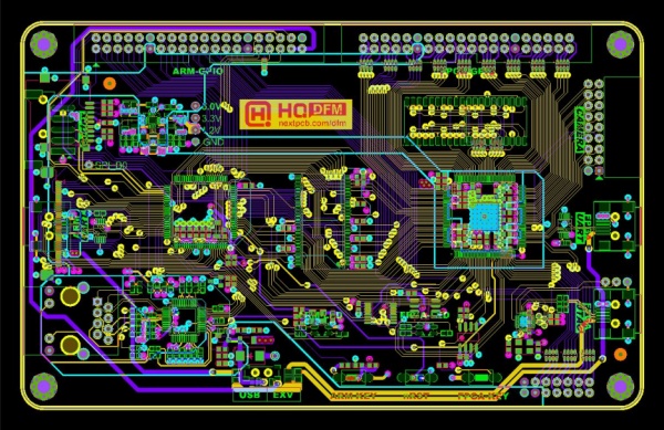
3. Leverage Manufacturer Feedback: Treat your fabrication partner as part of the design process. File feedback from DFM reviews often reveals hidden issues, like spacing violations or drill size conflicts, that simulations alone may not catch. NextPCB's automated DFM checks are a simple way to integrate this habit into every project.
> HQDFM Free PCB DFM Analysis Tool - Free Download - NextPCB
4. Document Every Iteration: Keep detailed notes on what worked, what failed, and what changed between versions. A well-kept design log not only helps you learn faster but also makes collaboration with peers or manufacturers smoother.
5. Test Under Real Conditions: Don't just validate signal flow, stress your prototype under realistic voltage, current, and thermal loads. This is often where weaknesses surface, and catching them early prevents costly surprises in later stages.
6. Fail Forward, Learn Fast: Mistakes aren't setbacks; they're feedback. The goal of prototyping isn't perfection, but rapid learning. Every failed iteration teaches you more about your design and the tools you'll need to succeed.
In practice, prototyping is less about avoiding mistakes and more about making them quickly, affordably, and constructively. With the right habits and the support of reliable fabrication partners like NextPCB, engineers and students can transform every prototype into a stepping stone toward better, more innovative circuits.
PCB prototyping is where creativity and engineering collide. It's the stage that transforms raw ideas into tangible circuits, exposing challenges in signal integrity, routing, or thermal behavior, but also offering opportunities for refinement and growth. For engineers and students alike, the prototype isn't just a test board; it's a learning platform, a validation tool, and a launchpad for innovation.
Modern techniques, like rapid fabrication, advanced materials, simulation tools, and DFM reviews, have made prototyping faster, smarter, and more reliable than ever. The real advantage comes from how well these tools are applied: documenting lessons, testing under real conditions, and iterating with purpose.
That's why choosing the right prototyping partner matters. Companies like NextPCB provide the speed, precision, and flexibility to turn sketches and schematics into working boards, removing barriers so innovators can focus on solving problems and pushing boundaries.
In the end, better prototypes don't just lead to better products. They lead to better engineers, better solutions, and a faster path from imagination to impact. The circuits of tomorrow start with the prototypes we build today. So build boldly, learn quickly, and partner wisely.
Abiola Ayodele: Broadcast Journalist & Tech Writer; Cooperate writer of NextPCB.
Specialize in technical writing, and editing, particularly in the areas of PCB design, semiconductors, cybersecurity, and emerging engineering technologies.
Still, need help? Contact Us: support@nextpcb.com
Need a PCB or PCBA quote? Quote now


 Surface

