
 NextPCB Capabilities
Printed Circuit Boards
NextPCB Capabilities
Printed Circuit Boards
 PCB Assembly
 Layer Buildup
 SMD-Stencils
 PCB Design-Aid & Layout
 Mechanics
 Quality
 Drills & Throughplating
 Factory & Certificate
 PCB Assembly Factory Show
Certificate
PCB Assembly Factory Show
Certificate
Support Team
Feedback:
support@nextpcb.com


This article is about the multi-layer circuit board design of Altium Designer suitable for beginners.
Before designing a multi-layer PCB circuit board, the designer needs to first determine the circuit board structure used according to the circuit scale, the circuit board size, and electromagnetic compatibility (EMC) requirements, that is, to decide whether to use 4 layers, 6 layers, or More layer circuit board. After determining the number of layers, determine where to place the internal electrical layers and how to distribute different signals on these layers. This is the choice of multilayer PCB stack-up basic. The laminated structure is an important factor that affects the EMC performance of the PCB board, and it is also an important means to suppress electromagnetic interference. This section will introduce the relevant content of the multilayer PCB board stack-up.
There are many factors to consider when determining the laminated structure of a multi-layer PCB board. From the perspective of wiring, the more layers, the better the wiring, but the cost and difficulty of board manufacturing will also increase. For manufacturers, whether the laminated structure is symmetrical or not is the focus that needs to be paid attention to when manufacturing PCB boards, so the selection of the number of layers needs to consider the needs of various aspects to achieve the best balance.
For experienced designers, after completing the pre-layout of components, they will focus on the PCB wiring bottlenecks. Combine with other EDA tools to analyze the wiring density of the circuit board; then synthesize the number and types of signal lines with special wiring requirements, such as differential lines, sensitive signal lines, etc., to determine the number of signal layers; then according to the type of power supply, isolation, and anti-interference The requirements to determine the number of internal electrical layers. In this way, the number of layers of the entire circuit board is basically determined.
After determining the number of layers of the circuit board, the next task is to rationally arrange the order of placement of the circuits of each layer. In this step, the main factors that need to be considered are the following two points.
(1) The distribution of special signal layers.
(2) Distribution of power layer and ground layer.
If the circuit board has more layers, more types of special signal layers, ground layers, and power layers will be arranged and combined. The more difficult it is to determine which combination is the best, but the general principles are as follows.
(1) The signal layer should be adjacent to an inner electric layer (internal power/ground layer), and the large copper film of the inner electric layer is used to provide shielding for the signal layer.
(2) The internal power layer and the ground layer should be tightly coupled, that is, the thickness of the medium between the internal power layer and the ground layer should be a smaller value to increase the capacitance between the power layer and the ground layer and increase the resonance frequency. Between the internal power plane and the ground plane
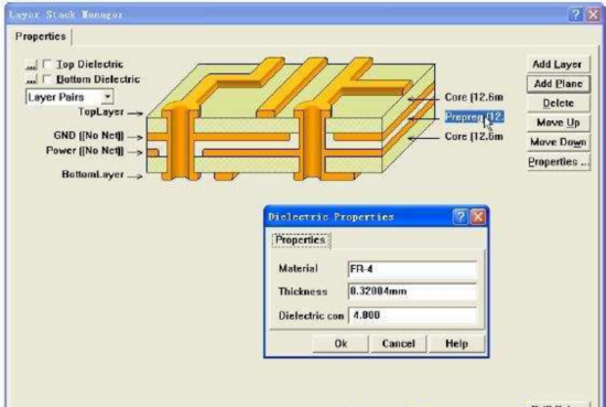
The thickness of the media can be set in Protel's Layer Stack-up Manager (r layer stack-up manager). Select【Design】
/[Layer Stack-up Manager...] command, the system pops up the Layer Stack-up Manager dialog box, double-click the Prepreg file with the mouse
This, pop up as shown in Figure 1. If the potential difference between the power supply and the ground wire is not large, a smaller insulating layer thickness can be used, such as 5mil
(0.127mm).
(3) The high-speed signal transmission layer in the circuit should be a signal intermediate layer and sandwiched between two inner electrical layers. In this way, the copper film of the two inner electric layers can provide electromagnetic shielding for high-speed signal transmission, and at the same time, it can effectively limit the radiation of the high-speed signal between the two inner electric layers without causing external interference.
(4) Avoid two signal layers directly adjacent to each other. It is easy to introduce crosstalk between adjacent signal layers, resulting in circuit function failure. Adding a ground plane between the two signal layers can effectively avoid crosstalk.
(5) Multiple grounded internal electrical layers can effectively reduce grounding impedance. For example, the A signal layer and the B signal layer use separate ground planes, which can effectively reduce common mode interference.
(6) Taking into account the symmetry of the layer structure.
The following uses a 4-layer board to illustrate how to choose the arrangement and combination of various sample board structures. For the frequently used 4-layer boards, there are several ways (from the tiny layer).
Obviously, Scheme 3 lacks effective coupling between the power layer and the ground layer and should not be adopted.
So how to choose between Option 1 and Option 2? Under normal circumstances, designers will choose option 1 as the structure of the 4-layer board. The reason for the choice is not that Option 2 cannot be adopted, but that the general PCB boards only place components on the top layer, so Option 1 is more appropriate. However, when components need to be placed on both the top and bottom layers, and the dielectric thickness between the internal power layer and the ground layer is large and the coupling is poor, it is necessary to consider which layer has fewer signal lines. For Option 1, there are fewer signal lines on the bottom layer, and a large-area copper film can be used to couple with the POWER layer; on the contrary, if the components are mainly arranged on the bottom layer, Option 2 should be used to make the board.
If the layered structure shown in Figure 1 is adopted, the power layer and the ground layer are already coupled. Considering the requirements of symmetry, scheme 1 is generally adopted.
After completing the analysis of the laminated structure of the 4-layer board, the following uses an example of the 6-layer board combination to illustrate the arrangement and combination of the 6-layer board and the preferred method.
Solution 1 uses 4 signal layers and 2 internal power/ground layers. It has more signal layers, which is conducive to the wiring work between components. However, the defects of this solution are also more obvious, which are manifested in the following two aspects.
Scheme 2 Compared with scheme 1, the power layer and ground layer are fully coupled, which has certain advantages over scheme 1, but Siganl_1 (Top) and Siganl_2 (Inner_1) and Siganl_3 (Inner_4) and Siganl_4 (Bottom)
The signal layer is directly adjacent, the signal isolation is not good, and the problem of prone to crosstalk has not been solved.
Compared with scheme 1 and scheme 2, scheme 3 has one less signal layer and one more internal electrical layer. Although the available wiring level is reduced, this scheme solves the common defects of scheme 1 and scheme 2.
Comprehensively speaking, scheme 3 is obviously the most optimized one. At the same time, scheme 3 is also a commonly used laminated structure for 6-layer boards.
2-4 days quick turn prototyping for multi-layer PCB
Through the analysis of the above two examples, I believe that readers have a certain understanding of the cascading structure, but in some cases, a certain plan cannot meet all the requirements, which requires consideration of the priority of various design principles.
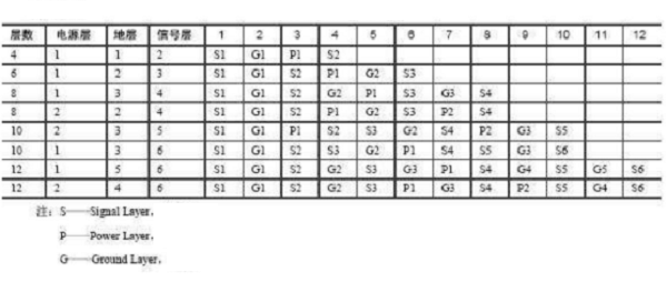
Unfortunately, because the board layer design of the circuit board is closely related to the characteristics of the actual circuit, the anti-interference performance and design focus of different circuits are different, so in fact, there is no determined priority for these principles for reference. But what is certain is that design principle 2 (the internal power layer and the ground layer should be tightly coupled) needs to be met first in the design, and if high-speed signals need to be transmitted in the circuit, then design principle 3 (high-speed signal transmission layer in the circuit) It should be the signal intermediate layer and sandwiched between two inner electrical layers) must be satisfied. Table 1 shows the reference scheme of the laminated structure of the multilayer board for the reader's reference.
Still, need help? Contact Us: support@nextpcb.com
Need a PCB or PCBA quote? Quote now


 Surface

