
 NextPCB Capabilities
Printed Circuit Boards
NextPCB Capabilities
Printed Circuit Boards
 PCB Assembly
 Layer Buildup
 SMD-Stencils
 PCB Design-Aid & Layout
 Mechanics
 Quality
 Drills & Throughplating
 Factory & Certificate
 PCB Assembly Factory Show
Certificate
PCB Assembly Factory Show
Certificate
Support Team
Feedback:
support@nextpcb.com


Laser cut the stainless steel foil to create an opening for each surface-mounted device on the board. After the template is properly aligned on the circuit board, apply solder paste to the opening (single pass with a metal wiper). When the stainless steel foil is separated from the board, the solder paste will remain and the SMD is ready to be placed. In contrast to manual welding methods, this process ensures consistency and saves time. You can add the PCB stencil to any PCB manufacturing order. Go to Nextpcb Quote to order and choose from a variety of template types and sizes to meet every requirement of your template.
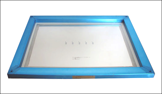
The framed SMT template or "glued" template is a laser cut solder paste template, which is permanently fixed in the template frame with mesh frame to tightly stretch the taut template foil in the frame. The framed template is designed for mass screen printing on printed circuit boards. The SMT template with frame has smooth hole wall, which can be used for below 16 mils and micro BGA. It has the following functions:
The frameless SMT template, also known as foil, is a laser cut solder paste template designed to work with a template tensioning system known as a reusable template frame. There is no need to permanently glue the formwork to the frame. The price of frameless template is much lower than that of framed template, which can save cost and provide excellent quality and performance. It has the following features and functions:
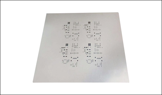
The prototype SMT template is a laser cutting template customized according to Gerber or CAD files to match the prototype PCB. These frameless solder paste molds are specially designed for manual printing. It has the following features and functions:
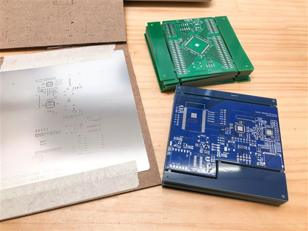
It is necessary to print solder paste on the pad of PCB before mounting surface mount components on the board. The stencil made of thin stainless steel is used as a screen for printing solder paste. If there is no template printer, align the pads on the circuit board with the holes on the template, and check the circuit board and template carefully to make sure they are aligned correctly. Then, fix the mold with adhesive tape.
For IC with 1.27mm spacing or 0.8mm spacing, this method can be used for alignment, but for narrow spacing pads (such as 0.5mm spacing or 0.4mm spacing), this alignment will become very difficult.
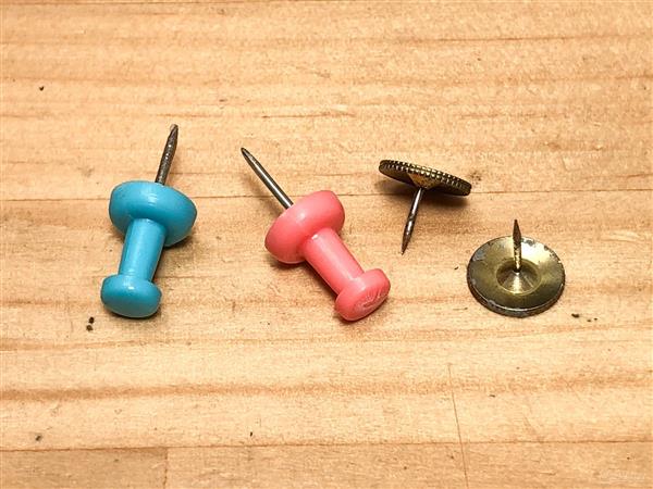
Diameter measurement, which is a simple way to align them using pins. Measure the diameter of the pin.
Creating a library
Create a library of holes for pins in kicad's footprint editor. Place a pad. Double click to open its properties.
Click the [local gap and settings] tab, solder mask gap: 1 mm
The library has been completed with a hole with a diameter of 1 mm and a solder mask hole with a diameter of 1 mm above it. Put the footprints just made on the four corners of the separated slide rail.

Still, need help? Contact Us: support@nextpcb.com
Need a PCB or PCBA quote? Quote now


 Surface

