
 Surface


Stacy Lu

 NextPCB Capabilities
Printed Circuit Boards
NextPCB Capabilities
Printed Circuit Boards
 PCB Assembly
 Layer Buildup
 SMD-Stencils
 PCB Design-Aid & Layout
 Mechanics
 Quality
 Drills & Throughplating
 Factory & Certificate
 PCB Assembly Factory Show
Certificate
PCB Assembly Factory Show
Certificate
Support Team
Feedback:
support@nextpcb.com


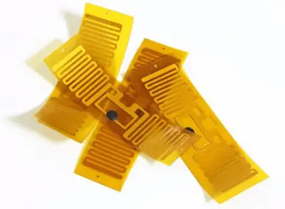
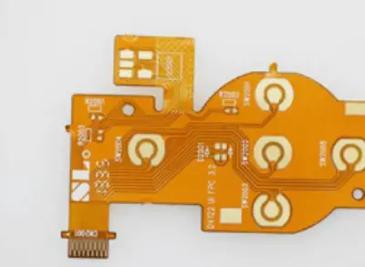
Flexible Printed Circuit Boards (Flex PCBs) have revolutionized modern electronics, enabling designs that fold, twist, and fit into ultra-compact, non-planar spaces -- from high-end wrist wearables to critical automotive sensors. However, transitioning from rigid boards to flexible circuits requires a shift in mindset. Designing a board that moves is fundamentally different from designing a rigid FR-4 board that stays static.
If you are still deciding which board type fits your project, see our comparison guide: Flex vs. Rigid vs. Rigid-Flex PCBs: Which One Do You Need?. For a broader introduction to flex circuit fundamentals -- structure, materials, and applications -- see our Flexible Printed Circuit Board overview.
For those ready to start designing, this guide covers the critical materials, mechanical layout rules, and cost factors you need to master to ensure your flex circuit is not only manufacturable but also reliable over its lifespan.
Unlike traditional rigid boards that rely on fiberglass-reinforced epoxy (FR-4) for structure, flex PCBs use flexible polymers as the base substrate. This fundamental difference allows the circuit to conform to specific housing shapes or endure repeated dynamic flexing during operation. While this offers incredible design versatility, it introduces new challenges around mechanical stress, tear resistance, and thermal management that every engineer must address before finalizing a design.
Selecting the right material is the first and most critical step in flex design. Your choice dictates the board's flexibility, thermal resistance, and overall cost. Unlike rigid boards, where FR-4 is the default, flex boards require you to balance mechanical properties against electrical performance.
| Material | Key Characteristics | Thermal Resistance | Relative Cost | Typical Application |
|---|---|---|---|---|
| Polyimide (Kapton®) | Excellent flexibility, chemical resistance, and thermal stability -- the industry standard | High (compatible with reflow soldering) | Medium-High | Industrial, medical, automotive, aerospace |
| Polyester (PET) | Good flexibility and electrical properties, but melts at high temperatures and cannot be reflow soldered | Low | Low | Membrane switches, low-cost consumer devices |
| LCP (Liquid Crystal Polymer) | Superior high-frequency performance with low moisture absorption | High | Very High | 5G antennas, high-speed data transmission |
"Kapton" is DuPont's brand name for polyimide film, and the two terms are used almost interchangeably in the flex PCB industry -- so much so that "kapton flex circuit" and "polyimide flex circuit" typically refer to the same material family. Polyimide film is favored over polyester (PET) for professional flex circuits for three practical reasons:
If your board needs to survive SMT assembly or a harsh operating environment, polyimide (Kapton) is effectively the default choice, and PET is reserved for low-cost, low-temperature applications such as membrane switches.
Modern high-reliability flex boards increasingly use adhesive-less base materials. By bonding copper directly to the polyimide core without an acrylic adhesive layer, you reduce total board thickness and improve both flexibility and long-term reliability -- particularly important for dynamic-flex applications, where every extra layer adds stress-bearing material at the bend point.
Expert Tip: For most general-purpose flex circuits requiring component assembly, polyimide offers the best trade-off between performance, manufacturability, and cost.
Before you commit a flex board to fabrication, run through this checklist. Each item addresses a mechanical or electrical constraint that does not exist in rigid PCB design:
| Consideration | Why It Matters |
|---|---|
| Application type: static or dynamic | Determines the bend radius multiplier, copper type, and layer strategy for the entire design |
| Substrate and copper selection | Polyimide with rolled-annealed (RA) copper is the standard choice for any design that will flex repeatedly |
| Bend radius vs. mechanical clearance | The calculated minimum bend radius must physically fit inside the housing or enclosure geometry |
| Trace routing through bend zones | Traces should cross the bend perpendicular to the bend line, with staggered layers to avoid the "I-beam" stiffening effect |
| Component and via placement | No vias, through-holes, or heavy components inside a bend zone -- move them to rigid or stiffened areas |
| Pad reinforcement | Teardrops and anchor pads prevent pads from lifting off the substrate under mechanical or thermal stress |
| Stiffener placement | Needed under connectors, BGAs, and heavy components to prevent solder joint fatigue |
| Coverlay and solder mask choice | Coverlay is generally preferred in bend areas; flexible solder mask can be used in flat, non-flexing zones |
| Panel utilization and shape | Irregular flex outlines reduce material yield and drive up unit cost -- worth reviewing with your fabricator early |
| Manufacturer capability check | Confirm minimum trace width/spacing, hole size, and coverlay tolerances with your fabricator before finalizing the layout |
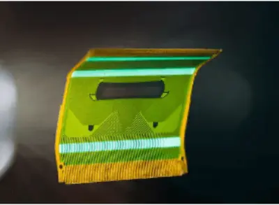
Designing for flex requires a "mechanical mindset." The copper on a flex board is thin and ductile, but it behaves differently under stress than on a rigid board. Ignoring these mechanical constraints is a leading cause of field failures.
Copper will crack if bent too sharply. To prevent this, follow minimum bend radius guidance based on the board's total thickness and how it will be used in the field. The table below reflects widely cited IPC-2223 industry guidance; always confirm exact multipliers with your fabricator's DFM documentation for your specific stack-up.
| Flex Type | Definition | Typical Minimum Bend Radius (x total thickness) |
|---|---|---|
| Static Flex (Install-to-Fit) | The board is bent once during installation and remains fixed for the product's life | 6x (single-layer) to 10-12x (multilayer) |
| Dynamic Flex | The board flexes continuously during operation (e.g., a printer head cable or a foldable-device hinge) | 100x (single-layer) up to 150-200x (multilayer) |
The gap between static and dynamic requirements is large -- roughly an order of magnitude -- because dynamic circuits must survive thousands to millions of flex cycles without fatigue cracking, not just a single installation bend. Using a static multiplier on a dynamic application is one of the most common and costly design mistakes in flex PCB engineering.
Flex substrates bond less aggressively with copper than rigid FR-4 does, so pads can peel off (delaminate) if pulled or heated too much.
Total flex thickness is the single most important input to the bend radius calculation above, so it is worth locking down early in the design process. As a reference, NextPCB's standard flex PCB manufacturing supports a finished thickness range of 0.1 mm to 0.45 mm, built up from the substrate, copper, adhesive (if used), and coverlay layers. Thinner constructions generally allow a tighter bend radius and better dynamic flex life, which is why adhesive-less, thin-copper builds are common in wearable and foldable-device designs.
A common misconception is that a flex board must be flexible everywhere. In reality, most flex boards are "hybrid" structures. Stiffeners are non-conductive mechanical supports added to specific areas of the flex circuit to provide a stable base.
| Material | Best Suited For |
|---|---|
| FR-4 | The most common choice for general component support |
| Polyimide | Used when you only need a slight thickness increase without adding much weight |
| Aluminum / Stainless Steel | Used when heat dissipation is critical, alongside mechanical support |
Engineers are often surprised to find that flex PCBs can cost 2-3x more than rigid PCBs at low volumes. Understanding the cost drivers helps you design more economically.
Based on NextPCB's manufacturing experience, avoiding these pitfalls can save you costly respins:
Designing a flex board involves a delicate balance between electrical performance and mechanical endurance. The process is more complex than rigid PCB design, but the ability to fit electronics into any shape provides a real competitive advantage for your product. For a broader look at flex circuit fundamentals and NextPCB's full manufacturing capability specifications, see our Flexible Printed Circuit Board guide, or explore our Flex & Rigid-Flex PCB manufacturing services.
Need Speed? Accelerate with NextPCB's Quick Turn Services
Time-to-market is critical. For engineers who need to validate designs fast, NextPCB offers a dedicated Quick Turn PCB Prototyping service tailored for flex circuits, bridging the gap between design and physical product with speed and precision:
Don't let fabrication challenges slow down your innovation.
Get an Instant Quote for Flex PCB Assembly Engineer Consultation
Start by defining your stack-up, materials (typically polyimide), and expected bend regions. Make sure the bend radius and layer structure meet both your electrical and mechanical requirements. Since flex areas are prone to stress, avoid placing vias and heavy components near these zones, and route traces with smooth, gradual curves to minimize stress concentration.
Copper traces in bend areas experience tensile stress on the outside of the bend and compressive stress on the inside. If the bend radius is too small or the routing is poor, this stress can crack the copper or delaminate the surrounding material. Follow IPC-2223 bend radius guidance for your application type and layer count, and route traces perpendicular to the bend axis to distribute stress evenly. Avoid right-angle turns and sharp trace corners inside flex zones.
The bend radius is the smallest radius a flex PCB can bend around without damage, and it depends on total thickness, layer count, and whether the bend is static or dynamic. Widely cited IPC-2223 industry guidance puts static bends at roughly 6× thickness for single-layer constructions (up to 10–12× for multilayer), while dynamic bends—circuits that flex repeatedly in normal operation—require roughly 100× thickness or more. Always confirm exact multipliers with your fabricator's DFM guidelines for your specific stack-up.
Sharp trace corners, stacking traces directly on top of each other in bend areas (the "I-beam" effect), and placing vias or heavy pads inside flex zones are the most frequent causes of failure. Route traces perpendicular to the bend axis, keep trace width uniform through flex regions, and stagger traces on different layers to avoid stress concentration.
Yes. Components, heavy pads, and vias in bend zones significantly increase the risk of mechanical failure. Vias are rigid plated features that do not flex with the surrounding material, which leads to cracking or delamination over repeated cycles. Keep these features outside bend regions, and use teardrop reinforcements or stiffeners to support traces and pads near high-stress areas.
Kapton is DuPont's brand name for polyimide film, so in everyday flex PCB terminology the two terms refer to the same material family. Polyimide/Kapton is preferred over polyester (PET) for professional flex circuits because it survives SMT reflow soldering, maintains its properties across a wide temperature range, and resists common assembly chemicals.
Finished flex PCB thickness commonly falls between roughly 0.1 mm and 0.45 mm, depending on layer count, copper weight, and whether the construction uses adhesive or adhesive-less bonding. Thinner builds generally allow a tighter bend radius and longer dynamic flex life.

Still, need help? Contact Us: support@nextpcb.com
Need a PCB or PCBA quote? Quote now

