
 NextPCB Capabilities
Printed Circuit Boards
NextPCB Capabilities
Printed Circuit Boards
 PCB Assembly
 Layer Buildup
 SMD-Stencils
 PCB Design-Aid & Layout
 Mechanics
 Quality
 Drills & Throughplating
 Factory & Certificate
 PCB Assembly Factory Show
Certificate
PCB Assembly Factory Show
Certificate
Support Team
Feedback:
support@nextpcb.com


It is a PCB constructed with three copper conductor layers. The layers of a 3-layer PCB appear to be represented by the conductive foil. Prepreg is the insulating layer to bind the various inner layers together for processing in pairs. The insulating substance consequently has at least three layers of conductive material. In this kind of PCB, the ground is shielding support for signals which is the most important term during design. Three-layer PCB is practical to align a ground layer with each signal layer due to the potential for high transmission rates in a circuit. It is frequently beneficial to restrict layer overlap, reducing overall expenses and system thickness. Additionally, power floors are positioned exceptionally near the ground levels. The layers include the following groups:
Since the distribution and location of the various layers vary from situation to situation, several solutions are available on the market. The cost influences the order of the various stages prepared to incur for the project, among other factors. In any case, board designers try to distribute the levels rationally according to their analytical purpose. In order to improve the reliability of the system's functioning, these lines disperse among several tiers due to their high-speed transmission rates.
The copper and insulator layers that make up a PCB help make a stack up before constructing the final layout of 3 layer PCB board. Maintaining a good stack up is quite tricky. Thus multilayer printed circuit manufacturers like Proto-Electronics, a professional network in Europe that focuses on cross-section components and quick prototyping of SMT printed circuits, must be at the forefront.
When the board has several layers, the ability to boost up the energy with cross-interference reduction, minimize electromagnetic interference, and facilitate high-speed communications. In addition to enabling we need to accommodate several electrical circuits on a single board through the various layers of the three-layer PCB board, the structure of the PCB stack-up design gives the following advantages:
The number of materials is beginning to play a more significant role now that multilayer PCBs are available, and the project is affected by the final cost. The construction of the simplest stack-up is possible using 3-layer PCBs before moving on to more complex ones requiring skilled sequential lamination. The designer is less likely to encounter "impossible" solutions the more freedom he has to deconstruct his circuit. The PCB overlapping processes include placing the copper and insulating layers that help make up a circuit. There is little doubt that the stack up to choose from significantly influences the board's performance in various ways.
There are several rules and requirements for keeping up a solid stack. Let us focus on a select few:
The final board's thickness is measured using the PCB standard. The nominal thicknesses of the copper clad laminate are 0.5, 0.7, 0.8, 1.0, 1.2, 1.5, 1.6, 2.0, 2.4, 3.2, and 6.4 mm. The nominal thickness of paper-based copper-clad laminates ranges from 0.7 to 1.5 mm. Printed circuit boards' materials and PCB thickness vary based on the standard, which has JIS, JPCA, IPC/JPCA, UL, and other standards. The PCB thickness includes the thickness of the board itself, as well as it involves the copper foil, the plating, and other components. The printed circuit board's material has an impact on it.
It is common to divide the typical copper thickness for a three-layer PCB into 1oz (35 mm), 2oz (70 mm), and 3oz (105 mm). The copper thickness will, of course, depend on the sort of board made. Copper is 2 oz thick and used in high-current switching power supplies. Signal transmission usually requires a thickness of 1 oz. In a three-layered board, the inner layer weighs 1/2 oz and the outer layer 1 oz. The size of the three-layer PCB signal voltage and current, as well as the PCB's intended usage, are the two main elements that decide the thickness of the copper foil used for 70% of the circuit board.
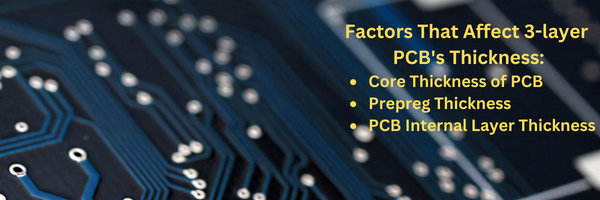
The PCB's thickness is influenced by several variables, including the environment, layer constraints, and the thickness of the copper element stacked up for the 3-layer PCB. The specification for three-layer PCB boards is significantly different from the norm. The traditional has a thickness of around 1.56mm. However, today's system is considerably more complicated since modern copper is exceptionally complicated, heavily weighted, and layered to the utmost extent possible with additional scopes. The new standard includes a thickness range of 2.3 to 3.2mm.
Why do we need three layered PCBs?
In this world of electronics and technology, there are a lot of complex devices based on instrumentation and circuit systems. Thus, this multilayer PCB has a broad scope, so the complex task is solved easily by utilizing different sorts of multilayered PCBs, including 3-layer. It will be much tough to complete the task in a single layer, so it plays much vital role in today's technological world. Additionally, the stack-up helps to solve such issues with single-layer PCB boards.
PCBs fabricates using three main types of materials:
This is the component of PCBs that utilizes as a gist element. It is a laminated glass-reinforced epoxy sheet. The epoxy used has water resistance and is flame retardant. It offers superior weight-to-strength ratios. This material has a very high level of tensile strength.
PTFE is a plastic substance utilized in high-speed, high-frequency applications because it offers no resistance. Due to its exceptional flexibility, PTFE is indispensable in applications requiring precise tolerances. Additionally, it helps in employing various sectors because of its light. Additionally, it is resistant to flames, potent physically, stable at all temperatures, and adaptable in use.
PCBs continue to employ conventional materials like copper, aluminum, iron, etc. Surface Mount Technology (SMT) may be used with these materials to integrate components. They also offer mechanical toughness. As a result, metal base PCBs have a substantially longer functional life.
The different materials used for the PCB design and fabrication all offer a variety of advantages and disadvantages. The material selects according to the application, the result needed, environmental factors, and any other constraints the PCB will face. You should choose the PCB materials depending on the expected results.
The components are required to design the PCB boards with the required software. They are the gist for developing any designs. Usually, there are similar components required for any PCB design. In addition, the 3-layer PCB boards comprise the following mentioned components:
For the design of the 3-layer PCB board, the sensor is one of the essential components. It can be a current, temperature, motion, etcetera. All the sensors have their respective features. The sensors in the PCB board are connected using the simulating software to sense the current, heat, or motion of any object respectively.
A printed circuit board's capacitor is a critical electrical component—the energy stored by this electrical component is released into a circuit. In a PCB, a capacitor is necessary. As a result, it only transmits alternating current and not direct current.
One of the most popular and likely most effortless to comprehend components on PCBs are resistors. Their purpose is to block the passage of electricity by converting electrical energy into heat.
A diode may accomplish numerous significant tasks. Its primary skill is the ability to determine the flow of electrical current. Only one direction of current flow is allowed through diodes. With the aid of an internal electric field, it is possible to direct current flow solely in the intended direction.
Vacuum-molded PCB transformers have an extremely high proof voltage as a result. They can be used as a power transformer on the PCB to offer electrical isolation or as an isolating or safety transformer to provide safe electrical separation for the input and output sides.
Here are the factors that will influence our material selection process:
There are specific differences between the various layered PCB boards. The main variation is the number of layers over them, which helps determine the efficacy and quality of any board.
Since the number of layers is higher in 6 layer PCB board compared to the 3-layer PCB, its manufacturing cost goes to be maximum. Along with that, the following methods to distinguish between the three-layer board and six layers can be:
If there is the presence of through holes only in the front part, not in the back, it notifies a 6-layer PCB board. Otherwise, it might be a 3-layer PCB of 4 layers.
Since the number of wires in six layers will be more significant than three-layer PCB, it will be more significant. However, on looking for individual layers, the six-layer comprises fewer compact wires than the three layers since it has more prominent space to spread out.
The advantages and disadvantages of the 3-layer PCB Vs. 6 layer PCB are mentioned below:
Pros for the 3-layer PCB are mentioned below:
Due to the increased circuit density, multilayer PCBs are more potent than simpler designs. They can operate at incredible speeds and have a more extensive working capacity, frequently required for the sophisticated electronics they power and enhance performance.
Multi-layer PCBs implies for more complicated devices with more circuits and components frequently. If it requires more circuits than would fit on a single board, you can add layers to increase the space. Multiple boards guarantee enough space for connections, making it perfect for more sophisticated systems. This complexity is necessary for devices like smartphones with a wide range of applications and sophisticated capabilities.
Due to their more detailed planning and production procedures, multilayer boards frequently have a more excellent quality than other types of boards. These boards need more expertise and sophisticated equipment to design and produce than do simpler components, increasing the probability that you'll receive a high-quality product. Many of these designs also have electromagnetic interference shielding and sophisticated regulated impedance characteristics, further enhancing performance.
A board with additional layers is thicker and, as a result, more robust than a single-sided PCB. This is another reason why expanding the size of a single layer is preferable to adding functionality through multiple levels. The boards can endure more challenging circumstances and frequently survive longer because of their increased resilience.
Multi-layer PCBs keep their low and tiny weight while achieving this increased resilience. Compared to other boards, they allow you to cram more functionality into a smaller area since layers may be stacked on top of one another. Reduced weight is also a result of this smaller size. For a single-layer board to perform as well as a multilayer board, it would need to be huge. You might even be able to duplicate it with several single-layer boards, but doing so would make your finished device bigger and heavier.
Using numerous PCB components, several connection points will be needed. Contrarily, multilayer boards are created to function with just one point of connection, simplifying the design of the electrical gadget and lowering weight. The multilayer printed circuit board is typically the better option when choosing between using many single-sided boards and simple ones.
Some of the disadvantages of the 3-layer PCB are mentioned below:
Creating and manufacturing multilayered circuit boards is more expensive than doing so for ones with only one or two layers. The cost increases because it takes more resources, time, and expertise. Please make sure a multilayer component's advantages exceed its disadvantages at all times. Keep using a single-layer PCB if having more than two layers is not essential.
Designing and producing multilayer boards is a more challenging and involved process than constructing single-layer boards. This implies requiring manufacturers and designers with advanced skills and specific tools. Additionally, you're more likely to run into problems along the way, particularly if you do not have the appropriate resources at your disposal.
Due to their specialized nature, not every manufacturer or supplier can consistently build or offer multilayer boards. Finding the ideal business to work with for designing, producing, or maintaining a board with many layers may be more difficult. Finding someone qualified to repair a board could also be more challenging if it requires repairs.
Multi-layer board design and production take longer than single-layer board design and production. There are other components to consider, and they must all be joined together to create a single board from the different layers. The complexity of these operations further lengthens the lead time. Multilayer PCBs might not be the best option if you need your boards created rapidly. Reworking may be time-consuming and don't perform without replacing parts; material costs increase with maximum mistakes during production or if you wish to modify the design.
Multi-layer PCBs are generally dependable, but their intricate design may make repairs more challenging if something goes wrong. It may be more difficult to pinpoint the issue if electrical component malfunctions or the board sustains physical damage since parts of the inside layers and the vias connecting them are not visible from the outside. Additionally, complicating and lengthening repairs are the board's many components.
In recent years, multilayer PCBs have become increasingly popular across various sectors. The growing need for small devices is what has led to its popularity. The most excellent option for industrial applications was PCB because of its lightweight and compact design.
Applications with a critical role for 3layer PCBs include:
Other names for them include home electronics. They cover a wide range of commonly used electrical devices. The communication tools among these home electronics include laptops and smart TVs. Additionally featured are smartphones and culinary gadgets. The ideal choice is a three-layer PCB since it makes the design more compact.
The medical sector requires electronic devices to function. Like other businesses, the industry embraced miniaturization. A three-layer PCB meets the exact specifications for the devices utilized in the medical sector. Their popularity and demand soared due to their compact size, strength, and lightweight design. The three-layer PCB is a design element used in medical devices like MRI and X-ray equipment. Numerous medical gadgets, including blood pressure monitors, contain PCB.
Three-layer multilayer PCBs are a durable alternative to other products on the market. Industrial electronics are not the same as the equipment utilized in the industrial setting. The 3-layer PCB exposes high humidity, dust, heat, and vibration. These gadgets work continuously throughout the day. As a result, the medical business demands Durability from its instruments. A 3-layer PCB satisfies the durability requirement.
With the use of technology and automation, our world is enormous. Therefore, 3-layer PCBs uses widely in computer-related equipment and their goods. Its practicality and decreased spacing qualities contribute to the computer industry's acceptance of it. The 3 layer PCB enables superior performance at a lower cost.
The 3-layer PCB can be used in the aircraft since it can withstand punitive situations and extremely high and low temperatures.
The design comes first in the production process. The first step is to plan the blueprint to accomplish everything mentioned in the design. This step is finished by designers using a program called Extended Gaber. A program is a superb tool that encodes all the information the designer needs. It translates the inner layer's component notation. It functions as an output format as well. The program also verifies each component to achieve a flawless design.
The design assessment suggests checking the design for flaws—checking each board component to prevent erroneous constructions.
The step of printing follows the assessment procedure. A plotter printer helps print the cinematic plot style using a copper board. It is an image of the board that is translucent.
The start of actual production happens at this stage. Pre-bonding the copper on the same laminates follows the printing of the pattern on the laminate—this aids in laying out the PCB's structure.
NextPCB provide PCB contract manufacturing services. Additionally, we offer inspection and testing services to guarantee the quality of each product. For our services, we adhere to worldwide norms and regulations. Additionally, we place a high priority on quick product delivery without sacrificing product quality. You can pick us for any service, including your 3-layer PCB. We deliver the highest caliber job while adhering to all requirements.
The stakes for high-performance and high-speed applications have increased due to changing technologies. As a result, the demand for multilayer PCBs like the three-layer board rises significantly. Building PCB solutions requires understanding the quality standards demanded by end customers. High-performing devices may be delivered more efficiently thanks to a layered architecture.
Still, need help? Contact Us: support@nextpcb.com
Need a PCB or PCBA quote? Quote now


 Surface

