
 Surface


Lolly Zheng- Sales Account Manager at NextPCB.com

 NextPCB Capabilities
Printed Circuit Boards
NextPCB Capabilities
Printed Circuit Boards
 PCB Assembly
 Layer Buildup
 SMD-Stencils
 PCB Design-Aid & Layout
 Mechanics
 Quality
 Drills & Throughplating
 Factory & Certificate
 PCB Assembly Factory Show
Certificate
PCB Assembly Factory Show
Certificate
Support Team
Feedback:
support@nextpcb.com


Introduction: What is Wave Soldering?
Wave Soldering is a highly automated mass soldering technology primarily used to reliably connect the leads of Through-Hole Technology (THT) components to a Printed Circuit Board (PCB). It works by briefly contacting the bottom of the flux-coated and preheated PCB with a wave of molten solder, completing the formation of all THT solder joints in a very short time. This process is a crucial step in high-volume electronics manufacturing for ensuring the mechanical strength and electrical continuity of components.
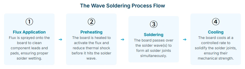
Table of Contents
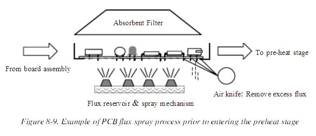
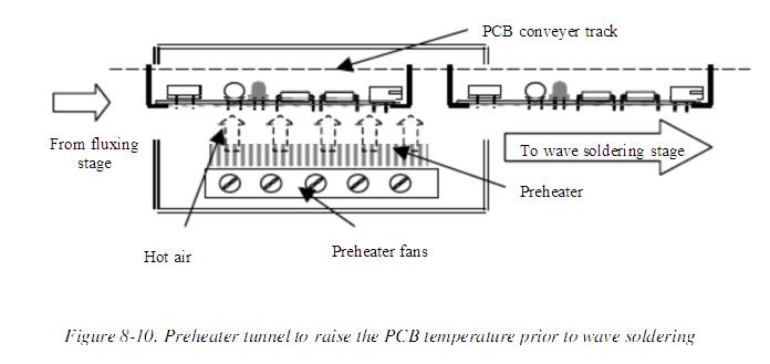
The wave soldering machine consists of four core functional areas. First is the Fluxing area, where flux is uniformly applied to the bottom of the PCB via spraying or foaming. Flux is the key chemical medium for successful subsequent wetting, as it removes oxides from the metal surface. Second is the Preheating area, whose purpose is to activate the flux and mitigate thermal shock. Next is the Soldering area, where the PCB bottom contacts the molten solder wave, and the solder flows to form the joints. Finally, the Cooling area is used to solidify the solder joints.
To address the increasing pin density and assembly complexity in modern PCB designs, contemporary wave soldering machines often use a Dual-Wave System. The dual-wave system effectively decouples the tasks of wetting and de-bridging, incorporating two types of solder waves:
> Recommend reading: Circuit Board Solder: Types, Temperatures & How to Choose (Reflow & Hand Soldering Tips)
Wave soldering is the dominant method for THT component soldering, primarily suited for components requiring high mechanical strength, high current carrying capacity, or long leads, for example, large connectors, relays, and certain electrolytic capacitors.
In Mixed Technology assemblies that include both SMT and THT components, the typical assembly sequence is to first complete all SMT component soldering via reflow soldering (Reflow), and then subject the remaining THT components to wave soldering. Since wave soldering processes the entire bottom of the PCB, it offers significant advantages in production efficiency, making it the most cost-effective choice for high-volume, relatively simple THT boards.
> Recommend reading: Reflow Soldering vs Wave Soldering: Difference and Process
However, if the PCB design is complex, component density is extremely high, or the board contains numerous heat-sensitive SMT components, traditional full-board wave soldering may be limited by thermal shock and bridging risks. In such cases, Selective Wave Soldering due to its precision in locally soldering specific joints becomes the preferred choice.
Start Your Project Now: Whether your board is high-density mixed technology or high-volume THT, get an instant quote now and experience the high-reliability, high-yield manufacturing and assembly services offered by NextPCB.
Wave soldering is a complex process involving the surface chemistry of molten metal and high-speed heat transfer dynamics. Understanding these fundamental mechanisms is prerequisite for controlling reliability.
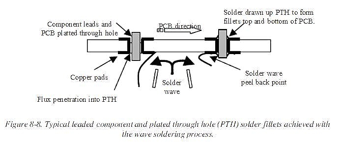
Wetting is the core of successful wave soldering. It describes the molten solder's ability to spread and form a metallurgical bond on the surface of the metal substrate (copper pads and leads). To form a reliable solder joint, the solder must first overcome the naturally occurring oxide layer on the metal surface and the high surface tension.
Flux plays a decisive role in this process. Activated during the preheat stage, the active agents in the flux efficiently remove metal oxides from the PCB pads and component leads, providing a clean metal surface for the solder. Additionally, flux reduces the surface tension of the molten solder, allowing it to flow and spread more easily.
Once effective wetting is achieved, Capillary Action drives the solder upward, filling the Plated Through-Hole (PTH). This capillary force is a direct result of the surface tension difference and is the physical guarantee for achieving a high Hole Fill. Therefore, the activity of the flux and the preheat temperature (to ensure the active agents work fully) are crucial for ensuring solder ascent.
The heat source for wave soldering comes from the molten solder wave at the bottom, and heat transfer is extremely fast, with contact time typically only 2 to 4 seconds. Heat is conducted to the PCB interior and topside through the leads, pads, and PTH barrel walls.
At the instant of soldering, there is a huge Thermal Gradient between the PCB topside and the bottom contact point with the solder wave. The board material's thermal mass significantly affects heat transfer efficiency. Thicker boards or PCBs with high copper weight (e.g., large power or ground planes) have a higher heat capacity. This means they need longer time or higher preheat temperatures to bring the temperature inside the through-hole and the component body up to the minimum threshold required for solder wetting. If heat input is insufficient, cold solder joints or insufficient hole fill may result internally.
Recommend reading: Fundamentals of PCB Thermal Design | NextPCB
The rapid temperature rise characteristic of wave soldering introduces an inherent risk of thermal shock. The PCB substrate (FR-4), copper conductors, and components (such as ceramics or silicon chips) have different Coefficients of Thermal Expansion (CTE/TCE). Rapid heating causes these materials to expand at uneven rates, generating concentrated stress at the solder joint and material interfaces.
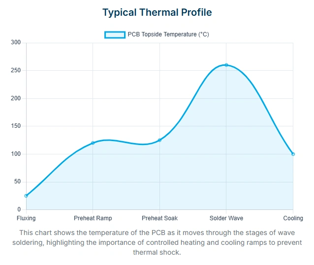
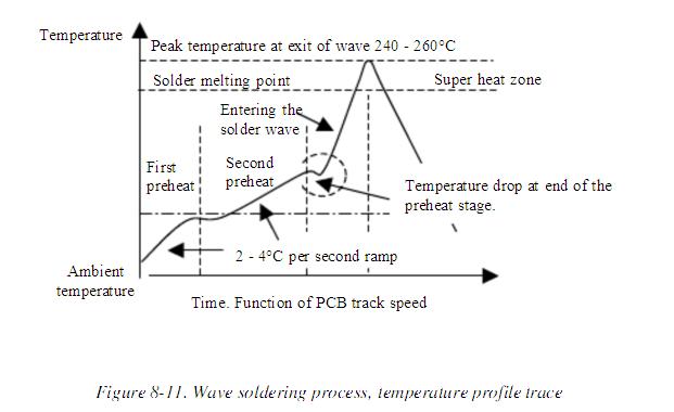
This stress concentration most severely affects two types of elements: first, the barrel walls of Plated Through-Holes (PTH), which are prone to fatigue cracks in the Z-axis direction; and second, large-mass components with low CTE, particularly ceramic capacitors larger than 1812. A single, extreme thermal shock event can initiate micro-cracks inside the ceramic component, while long-term thermal cycling will lead to fatigue failure of the solder joints due to alternating stress. Therefore, strictly controlling the ramp-up rate during the preheat stage (typically requiring less than 4°C/s) is necessary to keep the thermal strain rate within the material's tolerance, ensuring long-term reliability.
The stability of the wave soldering process depends on the balance and precise control of the following core parameters. Especially for Lead-Free solders (like SAC305), their higher melting point often results in a narrower parameter window compared to traditional tin-lead solder.
The selection and management of flux form the chemical foundation for ensuring successful wetting. High-reliability products tend to use alcohol-based, rosin-containing, halide-free fluxes (such as ROL0, ORL0) compliant with IPC J-STD-004 to ensure the electrochemical reliability of post-solder residues.
The preheat stage has three core objectives: activating the chemical activity of the flux, ensuring complete volatilization of solvents within the flux, and minimizing the risk of thermal shock.
> Recomend reading: Lead vs Lead-free Solder - An Ultimate Guide - NextPCB
The solder pot temperature must be set significantly above the melting point of the solder to ensure good flowability (low viscosity) and wetting ability. For lead-free SAC series alloys, the industry standard process temperature zone is approximately 25x–26x°C; this range is provided as an example only, and the final value must be validated with prototype thermal profiling and hole fill inspection. For lead-freeSAC alloys, the typical range is 250°C to 260°C. Insufficient temperature leads to poor wetting and inadequate hole fill; excessively high temperatures can cause component thermal damage and accelerate solder oxidation and dross formation.
Contact time refers to the duration the PCB solder joints are in contact with the solder wave, determined jointly by the conveyor speed and the length of the solder wave. Typical values range between 2.0 seconds and 4.0 seconds. Conveyor speed and wave length collectively determine the contact time. Typical contact time can start at approximately 2–4 s for DOE, with heavy-load/high-thermal-mass boards potentially requiring longer; this value is provided as an example only.
Engineering Trade-off: Contact time is the core contradictory parameter affecting hole fill and bridging probability. Extending contact time (e.g., more than 5 seconds, which may be needed for high-thermal-mass components) is beneficial for heat transfer and capillary action, ensuring hole fill. However, excessive time increases component thermal load and makes solder separation more difficult, raising the risk of bridging and icicles. Therefore, the conveyor speed must be precisely adjusted based on board thermal mass and component density to determine the optimal contact time.
Table 1: Key Wave Soldering Process Parameter Window (Lead-Free SAC305 Typical Values)
| Parameter | Typical Range | Function & Engineering Goal | Lower Limit Risk | Upper Limit Risk | Monitoring Point |
|---|---|---|---|---|---|
| Flux Solids | 2% – 5% (No-Clean) | Activates metal surface, aids wetting | Incomplete oxide removal, skips/non-wetting | Excessive residue, reliability/corrosion risk | Acid Value or Specific Gravity |
| Topside Preheat | 100°C– 150°C | Solvent volatilization, flux activation, reduces thermal shock | High thermal shock, flux not activated | Flux prematurely burnt off, component damage | Thermal Profile collection, Ramp Rate |
| Pot Temperature | 250°C – 260°C | Ensures solder flowability (Wettability) | Poor wetting, insufficient hole fill | Component thermal damage, accelerated solder oxidation | Constant temperature control, monthly composition analysis |
| Dwell Time | 2.0 s – 4.0 s | Ensures time for heat transfer and capillary action | Insufficient hole fill, skips/non-wetting | Component overheating, thermal shock, increased bridging | Conveyor speed/wave length calculation |
Systematic analysis of wave soldering defects is key to achieving high yields. Defects are often a direct manifestation of imbalanced process parameters, insufficient DFM, or poor material solderability.
| Symptom | Root Cause | Troubleshooting Sequence | DFM/Prevention |
|---|---|---|---|
| Bridging/Shorts | Solder wave height too high, leads too long, incorrect component orientation. | Check: Wave height, lead length, conveyor angle. | Orient components perpendicular to the wave; shorten lead protrusion length (<2.5mm); Solder Mask Dam design. |
| Insufficient Hole Fill | Insufficient topside preheat, contact time too short, low flux activity. | Check: Thermal profile, conveyor speed, flux acid value. | Extend contact time; optimize thermal relief pads; use high-activity flux; check board thermal mass. |
| Non-Wetting/Skips | Surface oxidation, poor component solderability, solder pot contamination. | Check: Flux activity, pad cleanliness, solder pot composition (Cu content). | Ensure uniform and sufficient flux coverage/activation; check component shelf life and solderability. |
| Thermal Shock Damage | Ramp rate too fast, insufficient preheating. | Check: Thermal profile for high-thermal-mass components (IPC-7530). | Strictly control ramp rate (<4°C); increase preheat temperature; use fixtures to protect sensitive components. |
Wave soldering yield is largely determined by the manufacturability (DFM) established during the PCB design phase, which requires design engineers to eliminate potential fluid dynamics defects through geometric layout.
Lead Orientation: The fundamental DFM requirement is that the pin arrangement of THT components (especially multi-pin ICs and connectors) must be perpendicular to the conveyor direction of the solder wave. This orientation ensures that the solder does not linger between adjacent pins when separating from the lead, significantly reducing the risk of bridging.
Solder Mask Dam: A small isolation strip formed by the solder mask, known as the Solder Mask Dam, must be retained between dense THT pads. The solder mask dam acts as a physical barrier, restricting the lateral flow of solder, making it a critical design element for preventing bridging.
Lead Protrusion Length: The length of the lead protrusion from the bottom of the PCB is a trade-off between geometry and thermals. The lead length must be sufficient (IPC recommends 0.7mm to 2.5mm) to ensure effective heat transfer and wetting, but excessive length (over 2.5mm) will significantly increase the likelihood of solder residue and bridging.
Shadowing Effect: The design must avoid placing small, low-profile components downstream of tall components (such as large capacitors or connectors). Tall components can obstruct the solder wave, creating a "shadow" zone behind them that leads to poor wetting or skipped joints for downstream components due to insufficient contact.
Thermally Sensitive and High-Thermal-Mass Components: For large ceramic components or high-thermal-mass components sensitive to thermal shock, if wave soldering cannot be avoided, the risk must be managed through strict DFM layout and process control. Ensure these components are placed in areas where the fixture/pallet provides the best thermal buffering, and measures are taken to control the ramp-up rate.
In mixed-technology boards, a fixture/pallet is often required to protect SMT components that have already been reflowed and sensitive areas on the board. The fixture not only provides mechanical support (especially for thin or thick boards to prevent warpage) but also acts as an isolation layer. A clearance of 5mm to 7mm must be left on the PCB edge for fixture gripping. For SMT components or non-soldered through-holes on the bottom side, a Temporary Solder Mask must be applied for shielding to prevent them from contacting the solder wave and contamination.
Free Design for Manufacturing (DFM) Review: Submit your PCB files and let our professional engineering team provide you with a free wave soldering DFM review, ensuring your design meets the highest reliability standards before manufacturing.
Upload & Quote Try HQDFM Online
Wave soldering as a mature technology must be compared with other THT soldering solutions to define its application boundaries.
| Feature | Wave Soldering | Reflow Soldering | Selective Wave Soldering |
|---|---|---|---|
| Applicable Components | THT (Through-Hhole), large connectors, high mechanical strength required. | SMT (Surface Mount Components), BGA/CSP. | Specific thermally sensitive areas on complex THT/mixed boards. |
| Solder Source | Molten Solder Bath. | Solder Paste pre-applied. | Small nozzle/solder pot, localized jet. |
| Thermal Stress Risk | Higher, risk of instantaneous full-board thermal shock. | Moderate, controllable thermal profile. | Localized, small Heat Affected Zone (HAZ), best thermal stress control. |
| Volume/Cost | High volume, highly cost-effective. | Extremely high volume, SMT production standard. | Medium-low volume, higher equipment and programming costs. |
Wave soldering uses a wave of molten solder to complete THT connections through brief contact; reflow soldering uses solder paste and multi-zone heating, primarily for SMT. Because wave soldering heat transfer is an instantaneous, localized process, it is inherently more challenging to control thermal shock and fluid dynamics (bridging) compared to reflow soldering.
Selective wave soldering uses a precise, localized small nozzle or dipping technology, soldering only predetermined areas with minimal Heat Affected Zone (HAZ). This makes it ideal for high-precision soldering on complex mixed-technology boards, protecting adjacent SMT components and thermally sensitive parts. Selective soldering offers higher quality and precision, but at the cost of higher equipment expense and slower point-by-point soldering speed. In contrast, wave soldering maintains an unparalleled advantage in speed and cost for processing high-volume boards with concentrated THT components.
If the PCB design contains a large number of temperature-sensitive leadless or highly integrated packages (such as BGAs, large QFNs), or if the THT pin density on the board makes geometric constraints (such as solder mask dams) impossible to meet, and the risk of bridging is extremely high, selective wave soldering should be considered. Furthermore, for applications with extremely stringent residue requirements (such as high-density avionics that do not permit cleaning), wave soldering should be used with caution, or a very low-residue flux should be selected.
The long-term stability and reliability of wave soldering depend on continuous online and offline monitoring.
Strict adherence to industry standards like IPC-7530 is mandatory for temperature profile acquisition. Engineers should use a minimum of three thermocouples (TCs): one attached through the PCB to the bottom to measure solder contact time, and the other two attached to the topside of the PCB to measure preheat temperature and ramp rate. The purpose of acquiring the thermal profile is to verify that the PCB has reached the minimum heat required to fully activate the flux and mitigate thermal shock before entering the solder wave, while ensuring the peak temperature and ramp rate are within the component's safe limits.
Flux Management: Due to solvent volatilization, flux activity changes over time. Solids content and Acid Value are common monitoring indicators, and their ranges must be calibrated according to vendor technical specifications and online inspection results. The Acid Value should be used as the main monitoring parameter because it directly reflects the concentration and chemical state of the active agent, making it more accurate than relying solely on specific gravity.
Solder Pot Purity: The molten solder in the pot is continuously contaminated by copper (Cu) impurities from the PCB, affecting solder flowability. High-volume production lines must regularly perform composition analysis to ensure copper impurity levels remain below the process threshold (typically < 0.1%) and periodically maintain or replace the solder bath material.
Final solder joint quality verification includes visual inspection (wetting angle, smoothness, absence of icicles/bridging) and the critical Hole Fill Rate determination (according to IPC-A-610 standard). For high-reliability applications, X-ray inspection can be used for non-destructive analysis to check for internal voids and hidden bridges. Cross-section analysis provides the most authoritative verification of the solder joint metallurgical structure (such as IMC layer thickness) and hole fill percentage.
Why is the preheat topside temperature typically controlled within a certain range?
How to choose between single wave and dual wave?
How should conveyor speed and contact time be adjusted for changes in board/copper thickness?
How to reduce bridging while ensuring hole fill?
Advice on thermal shock for ceramic/large-mass devices and recommended fixtures?
How should flux solids content/specific gravity be monitored and replenished?
Facing Assembly Challenges?

Still, need help? Contact Us: support@nextpcb.com
Need a PCB or PCBA quote? Quote now

