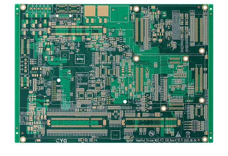
There does not seem to be a direct correlation between the PCB vias inserted into the solder mask and the copper. However, clogging with poorly performing solder resist can cause destructive results on the PCB. As a special technology of stencil printing, with the application and continuous development of SMT, the blocking technology of solder mask used in PCB manufacturing is also constantly developing.
Through-hole plugging has the following features:
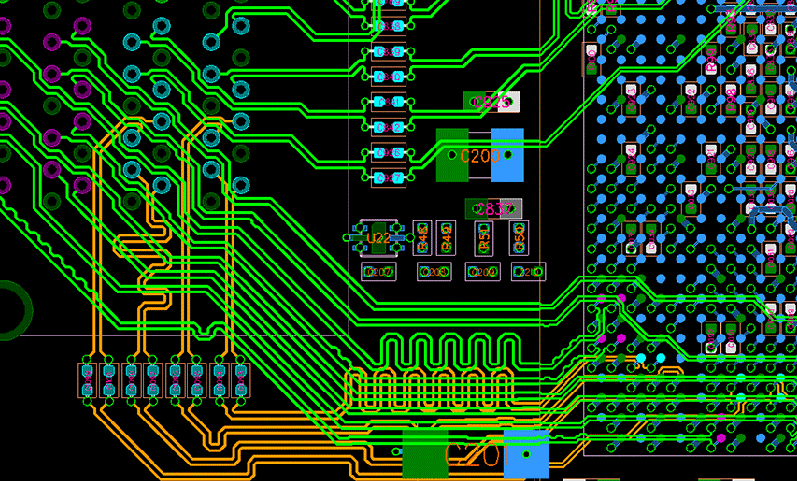
Among all the vias on the PCB, most of them do not need to be exposed except for component insertion vias, heat dissipation vias, and test vias. The blockage of the solder resist will prevent the flux or solder paste from being exposed to the component side through the through holes in the subsequent component assembly stage, because this may cause a short circuit. In addition, solder paste can be saved by applying solder mask blocking technology.
The solder mask plug hole meets the requirements of SMT and prevents the adhesive adhering to the surface of IC (integrated circuit) components from flowing through the hole.
The solder mask blocking technology prevents flux, chemicals, or moisture from entering the narrow space between the BGA component and the circuit board, thereby reducing the reliability risk caused by cleaning difficulties
Causes of blockage of the solder resist
1. One of the reasons for poor solder resist blockage is incomplete or insufficient solder resist blockage.
2. Incomplete or insufficient solder resist blockage refers to a situation where there is no solder resist oil at the top of the through-hole, and only a small amount of solder resist oil remains at the bottom.
3. Another example of incomplete or insufficient solder resist blockage shows that there is a solder resist on the left side of the through-hole, and the so-called air hole expands down the whole wall from the through-hole on the right side of the through-hole. When it approaches the middle part of the through-hole and produces a cross-section, it expands to the left side of the through-hole wall. The through-hole copper is almost broken at the intersection between the cross-section and the through-hole wall copper.
Causes of through-hole copper fracture or thinning
Once incomplete or insufficient solder resist blockage occurs, the micro-etching solution or acid solution may flow into the through-hole in the subsequent PCB manufacturing process. The through-hole is usually very small, with a diameter of less than 0.35 mm. When the solder resists clogging occurs, there is almost no solder resist oil left in the tent at the opening of the via, and there is a solder resist in the middle of the via or at the bottom of the via, so there is no general solution. The solution can only be hidden at the intersection of the solder mask and the through-hole wall, and cannot be eliminated, which will eventually cause the through-hole copper to break or become thinner.
Damage caused by broken or thin through-hole copper due to poorly implemented solder mask. When the copper becomes thinner inside the via, the resistance will reach the milliohm level. It cannot be tested using a two-wire measurement method so that defective products cannot be exposed.
1. If the electrical test cannot be exposed by exposing the copper fineness problem, the thin copper will be broken due to the high-temperature operation and the Z-axis expansion in the PCBA (printed circuit board assembly) phase containing solder. As a result, electronic products will not be fully functional, or their functions may become unstable when customers use them for a long time. If the through-hole copper is thin and not completely broken, it cannot be found by applying conventional inspection methods including AOI, AXI, and visual inspection. Once discovered, all products that will belong to the same production batch must be scrapped, causing huge losses.
2. In terms of copper fracture or circular fracture, PCB manufacturers can find it through electrical testing. Nevertheless, there is still a problem that the copper etching process through the micro-etching solution is so long that it does not occur until it reaches the customer stage. This means that only those customers who feel the electronic product's working condition is unstable can find the disconnection through copper. For example, when a customer finds that an electronic product suffers a black screen or is stuck, it may be caused by damage to the through-hole copper.
The solution to poor insertion of solder mask
From the perspective of engineering design
After the engineering department of the PCB manufacturing factory receives the PCB design documents from the customer, it should focus on the hole diameter and its requirements. Generally speaking, the hole diameter of the plugging hole should be less than 0.35mm, and should not be too large, because too large a hole will easily make the plugging incomplete or insufficient. Although customers have put forward requirements for through holes, they usually do not make specific regulations on the integrity of through holes. According to IPC regulations, there is no clear definition of insertion through integrity. According to the requirements set by the most extensive PCB manufacturers, it is most suitable for inserting through holes to achieve a filling degree of more than 75%.
From the perspective of improved solder mask blocking technology
So far, the PCB industry has mastered the following types of solder masks to be blocked by technology:
Technology #1 solder mask → solder mask printing (aluminum plate participates in the use of blocking and exhaust plates)
Technique #2 solder mask occurs at the same time as the solder mask is printed with oil.
Technology #3 resin plugging → solder mask printing
Technology #4 surface treatment → through plugging
As far as the integrity of the via filling is concerned, the first and third via filling techniques are recommended because both methods help to achieve high filling. However, they require a complicated manufacturing process of aluminum plates and exhaust plates. In addition, two or more printers are required for simultaneous printing, and the baking of the boards requires more time.
Technology #2 has high manufacturing efficiency, but it is difficult to control by fullness. This technique is not recommended because, according to the discussion earlier in this article, too low via fullness will cause via copper or via copper fracture.
Technology#4 is usually not applied, so it will not be discussed in the second half of this article.
Through-hole problems in electrical testing
The through-hole opening inspection indicates whether the through-hole copper is too thin or the resulting copper damage will cause an incomplete or insufficient through-hole blockage.
Electrical tests rarely pass copper thinning, but can explore the problem of round copper fracture. If a via is found during electrical testing, it can be used to verify whether it is caused by electroless copper plating, plating, or poor solder mask through plugging. After exploring the cause of the problem, you can list the corresponding measures.
From the perspective of solder mask or resin quality
The new product must be technically tested through the sealing flux oil and the sealing resin to ensure its quality. Then they should be used to participate in small-batch tests to further verify their performance and quality. As mentioned earlier in this article, too low a through-hole blocking the solder mask or resin blocking quality can cause some problems, such as pores. When the micro-etching solution enters the pores, the through-hole copper will be slowly etched away by the thin through-hole copper or through-hole copper fracture. Low cost will never compromise its quality.
The application of solder resist plays a key role in PCB manufacturing. The importance of through-hole filling is very important because it is related to the appearance of the product and is related to the quality of through-hole copper caused by incomplete or insufficient through-hole plugging. As a result, special attention should be paid to actual management. Specifically, standardized procedures should be followed. Production management should be perfect. Inspection standards should be clear to fully ensure the integrity of the through-holes.

 NextPCB Capabilities
 PCB Assembly
 Layer Buildup
 SMD-Stencils
 PCB Design-Aid & Layout
 Mechanics
 Quality
 Drills & Throughplating
 Factory & Certificate
 PCB Assembly Factory Show
Certificate
PCB Assembly Factory Show
Certificate
 NextPCB Capabilities
 PCB Assembly
 Layer Buildup
 SMD-Stencils
 PCB Design-Aid & Layout
 Mechanics
 Surface
 Quality
 Drills & Throughplating
 Factory & Certificate