The role of PCB
The function of the PCB is to provide a base for completing the first-level assembly of the components and other necessary electronic circuit parts to form a module or finished product with a specific function. Therefore, the PCB plays an integral role in the entire electronic product. Therefore, the role is often the first to be questioned when the function of electronic products fails. It is often the PCB. Figure 1.1 shows the hierarchy of electronic components.

The evolution of PCB
- 1. As early as 1903, Mr. Albert Hanson pioneered the use of the concept of "Circuit" (Circuit) to be applied to the telephone exchange system. It was made by cutting metal foil into circuit conductors and adhering it to paraffin paper and pasting a layer of paraffin paper. The prototype of the current PCB mechanism.
- 2. By 1936, Dr. Paul Eisner actually invented the PCB manufacturing technology and published a number of patents. Today’s print-etch (photo image transfer) technology is inherited from his invention.
PCB types and manufacturing methods
The diversification of the material-level manufacturing process is suitable for different electronic products and their special needs. The following summarizes some general different methods to briefly introduce the classification of PCB and its manufacturing method.
PCB type
- A. Classified by material
- a. Organic material: Phenolic resin, glass fiber/epoxy resin, Polyamide BT/Epoxy, etc.
- b. Inorganic material: Aluminum, Copper, Inver-copper ceramic, etc. are all of them, mainly for their heat dissipation function

- B. Differentiate between soft and hard finished products
- a. Rigid PCB
- b. Flexible PCB
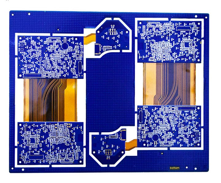
- c. Rigid-Flex PCB
- C. By structure
- a. Single panel
- b. Double panel
- c. Multilayer board
- D. According to the purpose of communication/consumable electronics/military/computer/semiconductor/electrical test board, there is another kind of injection-molded three-dimensional PCB because it is less used, so I won’t introduce it here.
Introduction to PCB manufacturing methods
- A. Subtraction
- B. Additive method can be divided into semi-additive and full-additive methods
- C. There is other advanced manufacturing processes that have been extended in response to the changes in IC packaging. This CD only mentions but does not introduce them in detail. Because many of them are confidential and not easy to obtain or are not mature enough. This CD uses the traditional negative multi-layer board manufacturing process. Introduce each process in a simple way for the main axis and discuss the future PCB trend with the concept of advanced technology.
 PCB Assembly
 Layer Buildup
 Online Tools
 PCB Design-Aid & Layout
 Mechanics
 SMD-Stencils
 Quality
 Drills & Throughplating
 Factory & Certificate
 PCB Assembly Factory Show
Certificate


