BGA is a commonly used component on PCB, usually CPU, NORTHBRIDGE, SOUTHBRIDGE, AGP CHI P, CARD BUS CHIP... etc. Most of them are installed. In short, 80% of high-frequency signals and special signals will Will be pulled from this type of package. Therefore, how to deal with the routing of the BGA package has a great impact.
Small parts usually surrounding the BGA can be divided into several categories according to their importance:
- 1. bypass.
- 2. clock terminal RC circuit.
- 3. Damping (appears in the form of series resistance and row group; for example, memory BUS signal)
- 4. E MI RC circuit (appears in the form of damping, C, pull height; for example, US B signal).
- 5. Other special circuits (special circuits added according to different CHIP; for example, the temperature sensing circuit of CP U).
- 6. Small power circuit groups below 40mi l (appear in C, L, R, etc.; this kind of circuit often appears in AGP CHIP or CH with AGP function to separate different power groups).
- 7. Pull low R, C.
- 8. General small circuit group (appears in R, C, Q, U, etc.; no wiring requirements).
- 9. pull height R, RP.
The circuits of items 1 to 6 are usually the focus of placement, and they will be arranged as close as possible to the BGA, which requires special treatment. The importance of the seventh circuit is next to BGA. Items 8 and 9 are general circuits, which are signals that can be connected.
Compared with the priority of the importance of small parts near the BGA, the requirements on ROUTI NG are as follows:
- 1. bypass => When the same side as CHIP, directly connect CHI P pin to bypass, and then pull out a bypass to connect via to plane; share the same via with BGA's VCC and GND pin, The cable length should not exceed 100mil.
- 2. clock terminal RC circuit => wire width, wire distance, wire length, or package GND requirements; the wiring should be as short as possible, smooth, and try not to cross the VCC points
- 3. damping => cable width, line spacing, line length, and packet routing requirements; the routing should be as short as possible, smooth, one set of cabling, no participation
- 4. E MI RC circuit => cable width, line spacing, parallel running line, package GND, and other requirements; completed according to customer requirements.
- 5. Other special circuits => cable width, package GND or wiring clearance requirements; completed according to customer requirements.
- 6. Small power circuit groups below 40mi l => cable width and other requirements; try to complete the surface layer as much as possible, and reserve the inner space for the signal line so that the power signal passes through the layer in the BGA area, causing unnecessary interference.
- 7. Pull low R, C => no special requirements; smooth wiring.
- 8. General small circuit group => no special requirements; smooth wiring.
- 9. pull height R, RP => no special requirements; smooth wiring.
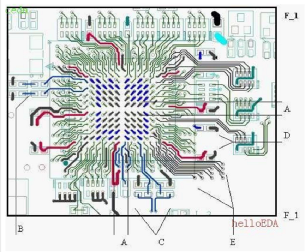
In order to more clearly explain the processing of the routing of BGA parts, a series of icons will be described as follows:

- A. Divide the BGA from the center with a cross, and VI A hits the upper left, lower left, upper right, and lower right directions respectively; the cross can be adjusted asymmetrically due to the wiring.
- B. The clock signal cable width and line distance requirements, when the R and C circuits are on the same side as the CHIP, please try to deal with the above diagram as much as possible.
- C. Please run the USB signal in parallel at both ends of R and C.
- D. Bypass try to connect the CHIP pin to the bypass and then enters the plane. Unable to receive the bypass, please get off the plane nearby
- E. For the signal of the BGA component, pull the outer three circles outwards, and keep the original set line width and line spacing; VI A can be placed in the part entity and 3MM placement forbidden interval. If the wiring has no level requirements, it can be extended without restriction. Pull the inner circle inward or VI A hits between PIN and PIN. In addition, the BGA is pulled out with the surface layer to reduce the number of VIA in the corners.
- F. The signal of the BGA component should be pulled out as far as possible in a radiation pattern; avoid the Bypass as close to the power pin as possible.
Because the BGA signal has regular leads and VI A, the ground conduction is sufficient.
The BGA routing recommendations made above have the following effects:
- 1. Regular leads are beneficial to the processing of special signals so that all wiring layers except the surface layer can be completed with the required line width and line spacing
- 2. The VCC and GND inside the BGA will therefore have better continuity.
- 3. The cross dividing line in the center of the BGA can be used; when the BGA has more than one internal power source and it is not easy to cut the VCC layer, it can be processed in the wiring layer (source supply side. Or the CLOCK of the BGA itself, or other large line widths) , Line distance signals are routed in the forward direction.
- 4. Good BGA wiring and placement can minimize the interference of BGA's own signal.

 NextPCB Capabilities
 PCB Assembly
 Layer Buildup
 SMD-Stencils
 PCB Design-Aid & Layout
 Mechanics
 Quality
 Drills & Throughplating
 Factory & Certificate
 PCB Assembly Factory Show
Certificate
PCB Assembly Factory Show
Certificate
 NextPCB Capabilities
 PCB Assembly
 Layer Buildup
 SMD-Stencils
 PCB Design-Aid & Layout
 Mechanics
 Surface
 Quality
 Drills & Throughplating
 Factory & Certificate