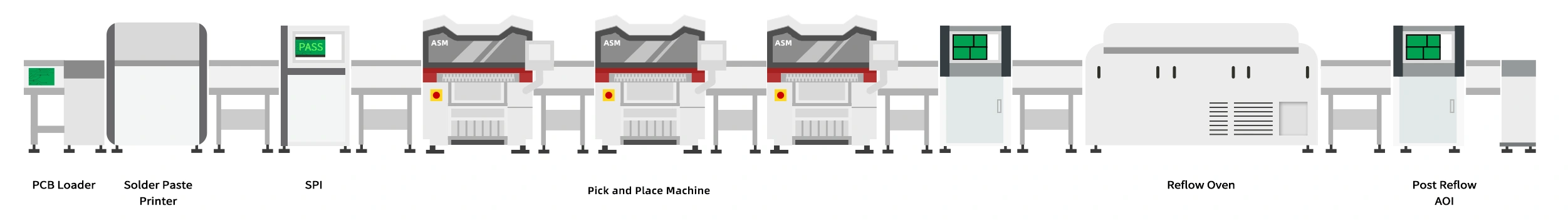
1. Pre-Production Preparation
The first step in SMT isn’t hitting “start,” but meticulous preparation—this stage directly determines the precision of everything that follows.
Document review: Engineers carefully cross-check the PCB layout, BOM, and Gerber files to ensure pad locations and package footprints match the design—avoiding “millimeter off, miles wrong” errors. > What is IPC Standard to PCB Layout Design?
Incoming material inspection: Resistors, capacitors, ICs, etc. undergo visual checks (damage, pin oxidation) and parameter verification (ohmic value, capacitance, model) to keep sub-standard parts off the line.
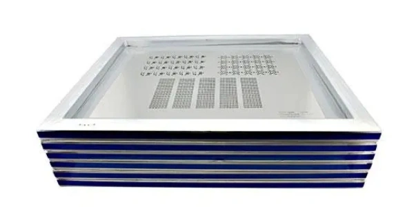
Stencil fabrication: The stencil is customized to pad geometry (typ. 0.12–0.15 mm thick). Aperture accuracy directly dictates print quality—it’s essentially the “soul” of solder paste printing.
> Recommend reading: PCB Assembly Drawings: Boost PCBA Manufacturing Efficiency & Reliability
2. Core Processes
Action #1: Solder Paste Printing
SMT assembly begins with solder paste printing that intends to put a correct quantity of solder paste onto a pad on which parts will certainly be soldered. This step is like applying “glue” for the PCB—depositing the right amount of solder paste onto the pads so that, during reflow, each SMD forms a reliable electrical connection with sufficient mechanical strength.
Mount the PCB on the printer table and align the stencil precisely to the pads. With the squeegee set at ~45°, sweep at a constant speed to transfer the solder paste (a mix of alloy powder and flux) through the apertures onto the pads, targeting a deposit thickness of 0.10–0.20 mm. After printing, post-print AOI scans for insufficients, skips, and bridging to ensure a pristine “base layer.”
> Recommend reading: Printed Circuit Board Basics: From Design to Final Artwork
The high quality of solder paste printing is mostly identified by 3 aspects: solder paste problem, scuffing angle, and also scuffing rate.
Excellent quality can never ever be gotten by SMT constructed PCBs unless solder paste is correctly kept and also used. Solder paste needs to be kept in a refrigerator to be kept in a reduced temperature level as well as its temperature level ought to be recouped to space temperature level before its application on SMT making line. In addition, the exposed solder paste needs to be consumed in 2 hrs. Aside from solder paste condition, solder paste printer specifications need to be effectively established, which is specifically real for scratching angle and also rate because both celebrations are very closely relevant with the particular quantity left on the pad.
When designing a stencil, two key ratios must be strictly controlled:
- 1. Area Ratio: The ratio of the stencil opening area to its sidewall area, calculated as Ra=Aperture Wall AreaAperture Area. An area ratio greater than 0.66 generally ensures smooth solder paste release, preventing clogging. For fine-pitch components, special aperture shapes (such as "home-plate" or "window-pane") can be designed on the pads to optimize the solder volume and prevent bridging.
- 2. Aspect Ratio: The ratio of the stencil opening width to its thickness, calculated as Ar=Stencil ThicknessAperture Width. An aspect ratio greater than 1.5 is generally recommended. When the aspect ratio is too small, the surface tension of the solder paste can cause it to stick to the hole walls, resulting in insufficient print volume.
The settings of the printing machine are also crucial, as they determine the physical behavior of the solder paste on the stencil:
- Printing Speed: The speed of the squeegee affects how the solder paste rolls on the stencil. A speed that is too fast may prevent the paste from fully filling the openings, while one that is too slow may cause excessive paste slump.
- Squeegee Pressure: The pressure must be moderate. Too little pressure can leave residual paste on the stencil surface, while too much pressure can "scoop out" the paste from the openings, resulting in insufficient deposition. Squeegee pressure should be calibrated based on the squeegee length and paste viscosity.
- Separation Speed: The speed at which the PCB separates from the underside of the stencil. A slow and controlled separation speed is vital to prevent the solder paste from forming "tents" or "smears" due to pulling, ensuring the integrity of the printed paste shape.
*Printing Process Control Points:
- Printer parameters: print speed 30–50 mm/s, squeegee pressure 1.5–2.5 kgf/cm², separation (snap-off) 0.1–0.3 mm, and cleaning frequency every ~2 hours.
- Solder paste management: select the paste type per product requirements (e.g., lead-free SAC), and use within its shelf life (typically ~6 months).
- Stencil quality: confirm stencil thickness (e.g., 0.12 mm) and aperture dimensions match pad design and meet spec.

Action #2: Solder Paste Inspection (SPI)
Solder paste assessment by itself is an optional method to decrease price due to the fact that it's far better to lower solder problems today than to capture them later on.
SPI is not a must-be action in SMT assembly however with it used it's beneficial to lower your production expense and also to boost the top quality of items. Besides, many flaws in SMT assembly originate from solder paste printing as well as if they can be figured out as well as handled a very early stage, the hazards perhaps bring about problems in later phases of production will certainly be reduced or perhaps removed. SPI maker includes 2 kinds: 2D as well as 3D. PCBCart has a 3D SPI maker in the workhouse to give far better evaluation solutions to clients.
Action #3: Chip Mounting
Chip installing plays a core duty in SMT assembly procedure. In practice, placement is performed manually or by pick-and-place (P&P) machines to locate SMDs precisely on pads that have solder paste or adhesive applied.
Manual placement suits prototypes and small/medium runs and the R&D stage. It’s easy to operate and cost-effective, but throughput and quality depend heavily on operator skill.
Machine placement is ideal for larger volumes and tight lead times. The chip mounters vary from each various other largely in regards to rate as well as placing capacity.
Some tiny parts are typically put by high-speed chip mounters that can position them swiftly to make those parts promptly stuck to the solder paste on the pad. P&P machines use vacuum nozzles to pick components (down to 0402 capacitors—sesame-seed sized) and a vision alignment system (accuracy to ±0.01 mm) to register both the component and PCB coordinates. Following the placement program, the head gently but precisely sets each part onto its pads to avoid damaging pads or components. High-speed chip-shooters can place tens of thousands of CPH, while high-accuracy placers specialize in BGA, QFP, and other complex packages to ensure tight lead-to-pad registration.
Nevertheless, huge parts such as BGAs, ICs, ports, and so on are normally positioned by multi-function chip mounters that perform at a fairly reduced rate. Regarding those parts are worried about, positioning does issue. It takes even more time to attain placement before chip installing, which is why the rate of multi-function chip mounter is a lot less than that of high-speed chip mounter. Additionally, a few of the elements made use of in multi-function chip mounter do not rely upon tape on the reel while some on tray or tube as a result of the constraints of dimension.
Component Placement
Best Practices for Handling Moisture-Sensitive Devices (MSDs) Moisture-Sensitive Devices (MSDs) are components whose packaging materials easily absorb moisture from the air. When these components pass through the high temperatures of a reflow oven, the absorbed moisture rapidly vaporizes and expands, creating enough vapor pressure to cause delamination, cracking, or even package rupture inside the component or between layers. This phenomenon is known as the "popcorning effect." This damage is often invisible but can lead to component failure. To prevent such issues, the industry widely follows the IPC/JEDEC J-STD-033 standard, which provides detailed guidelines for the handling, packaging, transport, and use of MSDs. The core protocols include:
- 1. Receiving and Inspection: Upon receiving MSDs, check their Moisture Sensitivity Level (MSL) labels and sealing dates on the packaging. MSL levels range from 1 (least sensitive) to 6 (most sensitive), with different levels corresponding to different floor life times.
- 2. Dry Storage: Unopened MSDs should be stored in a dry environment, such as a nitrogen cabinet or a low-humidity dry box, to maintain the integrity of their vacuum-sealed packaging. Once the package is opened, the component's floor life begins.
- 3. Floor Life Management: Floor life is the maximum amount of time a component can be exposed to a specified temperature and humidity environment. For example, an MSL Level 3 component has a floor life of 168 hours. If this time is exceeded, the component must be baked to remove the moisture.
- 4. Baking Treatment: When an MSD's floor life expires or its packaging seal is broken, it must be baked to restore its dry state. A typical baking temperature and time is 125°C for several hours. Baking is a necessary step to remove moisture, but it must be done under controlled conditions to avoid thermal stress to the component.
*Placement Control Points:
- Component orientation: verify polarized parts (e.g., electrolytic capacitors, diodes) are oriented correctly to avoid reversals.
- Placement speed: tune by package type (e.g., use medium speed for 0402 to avoid part fly-off).
- PCB warpage: keep ≤ 0.5 mm to prevent placement offset.
Action #4: Visual Evaluation + Manual Component Placement
After chip placing, it's required to accomplish aesthetic evaluation to make sure that reflow soldering can be greatly made certain to be without flaws. The leading concerns to be learned in this action consist of misplacement, missing out on components, and so on. The flaws are incredibly tough to be managed as soon as reflow soldering is done since they will certainly be sturdily repaired onto PCB. Because of this, items' dependability will certainly drop, and also manufacturing prices will certainly climb also.
On the other hand, some elements can be put straight by hand in this action, consisting of some huge elements, DIP elements, or those that can not be put via chip mounter as a result of some factors.
Action #5: Reflow Soldering

Once populated, the PCB enters the reflow oven and passes through four zones:
- Preheat (100–150 °C): gradual ramp to evaporate paste solvents and prevent thermal shock.
- Soak (150–180 °C): activate flux and remove oxides on pads and leads.
- Reflow (220–250 °C): solder alloy melts and forms joints, bonding components firmly to the PCB.
- Cooling: rapid cool-down to solidify joints and increase mechanical strength.
In the process of reflow soldering, solder paste is thawed to create IMC (Intermetallic Substance) to attach element pins as well as the board. The temperature level account adhered to in the process of reflow soldering procedure covers preheating, temperature level surge, reflow as well as air conditioning.
Take lead-free solder paste SAC305 as an instance, its melting point is roughly 217 ℃ so the solder paste can not be remelted unless the temperature level of the reflow soldering stove is greater than 217 ℃. Moreover, the greatest temperature level of the reflow soldering stove should not be greater than 250 ℃, or a lot of elements can not be thawed because of their incapability to hold up against such heat.
In fact, temperature level account setup establishes reflow soldering top quality and also helps in reducing manufacturing expense. Hence, it's far better to discover a knowledgeable SMT assembler as a CENTIMETERS (Agreement Supplier) that is totally knowledgeable about components affecting SMT soldering top quality and also renovation actions. All the components will certainly lead to manufacturing price being reduced.
Recommended SAC305 Lead-Free Solder Paste Reflow Profile:
SAC305 is a common lead-free solder paste (composition: 96.5% Tin, 3% Silver, 0.5% Copper), with a liquidus temperature of 217°C. Based on this, the following is a typical reflow profile setup recommendation:
- Preheat Zone: 150-180°C, for 60-90 seconds.
- Soak Zone: 180-217°C, for 60-120 seconds.
- Reflow Zone (TAL): Above 217°C, for 45-90 seconds.
- Peak Temperature: 235-245°C.
- Cooling Rate: 2-4°C/second.
This profile design accounts for the high melting point of SAC305, extending the preheat and soak times to ensure a uniform temperature across the entire board, thus effectively avoiding poor soldering due to temperature differences.
Reflow is a critical SMT step; a proper temperature profile is key to joint quality. An improper profile can cause insufficient wetting, cold joints, tombstoning, and excessive solder balls, degrading product quality.
*Reflow Control Points:
- Profile: match the curve to the paste’s characteristics (e.g., lead-free requires a higher peak).
- Oven airflow: hold pressure at 5–10 Pa for uniform temperature.
- Conveyor speed: adjust to oven length (e.g., 3 m oven → 0.5–1 m/min).
>SMT Assembly Quote
Action #6: AOI (Automated Optical Inspection)
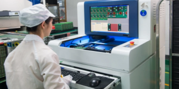
Already, elements have actually been repaired onto PCB after reflow soldering, which implies that the important part of the job worrying SMT assembly has actually been finished. Nonetheless, the setup boards can never ever be straight made use of in end products unless enough examination and also evaluation have actually been made.
The efficiency of solder joints can be double-checked with the application of AOI that can reveal defects such as cold/dry joints, oversized/undersized fillets, tombstoning, skew, missing components, misplacement/misalignment, solder bridging, and insufficient solder, with image-comparison accuracy up to 99.9%.
*Where to place AOI in the line
Although AOI can be deployed at multiple points—and each position excels at catching specific defect classes—the system should be placed where it can surface and correct the largest number of issues as early as possible. Three common placements are:
(1) After solder paste printing.
Typical print defects include:
- A. Insufficient paste on pads
- B. Excess paste on pads
- C. Poor paste-to-pad registration
- D. Paste bridging between pads
(2) Before reflow.
Inspection is performed after placement (components seated in paste) and before the PCB enters the oven. This is a classic position because it catches most defects from printing and placement. The quantitative process-control data gathered here helps calibrate high-speed chipshooters and fine-pitch placers. Use it to tweak placement parameters or indicate when a placer requires calibration—supporting robust process tracking.
(3) After reflow.
Inspection at the final SMT step is currently the most popular choice because it can detect all assembly errors. Post-reflow AOI provides the highest confidence, identifying defects originating from printing, placement, and the reflow process.
Action #7: AXI (Automated X-ray Inspection)
For packages with hidden joints (e.g., BGA, CSP), X-ray radiography evaluates solder joint quality by visualizing joint thickness, shape, and density/void distribution. These indicators reflect solder quality, including opens, shorts, voids, blowholes, internal bubbles, and insufficient solder, and they support quantitative analysis. AXI leverages the penetrating power of X-rays to test what optics can’t see.
AXI supplements AOI by exposing some issues more clearly and directly. It isn’t mandatory after reflow, but quality-focused assemblers deploy AXI to meet stringent OEM reliability requirements.
X-ray evaluation is a supplement to AOI given that it can suggesting some issues extra plainly as well as straight. It's not a must-be step after reflow soldering. Nonetheless, as long as the SMT assembler cares extra regarding items' top quality as well as dependability, an X-ray examination device will certainly be most definitely put on satisfying the extensive needs of some OEMs for the achievement of greater effectiveness.
Action #8: ICT or Functional Testing & Manual Rework
ICT (In-Circuit Test)
Then we go to ICT—bed-of-nails, contact-based testing—is one of the most fundamental production tests thanks to its strong fault-isolation capability. The PCBA is placed on a custom bed-of-nails fixture; spring probes contact component leads or dedicated test pads. Because the fixture touches all relevant nets, both analog and digital devices can be tested individually, and failing parts are rapidly diagnosed.
The objective of ICT is to examine whether opens up and also shorts are readily available in the circuit as well as to reveal some problems of some parts by gauging resistance, capacitance as well as inductance. Consequently, parts are evaluated to guarantee their high performance after reflow soldering.
Feature examination is a supplement of ICT given that ICT can just examine the opens up and also shorts on bare board yet the features of assemblying PCBs stop working to be evaluated. For that reason, the features of set up PCBs ought to be checked via feature examination in order to keep the high integrity of end products.
Manual rework
Boards flagged as defective are reworked using a hot-air gun or soldering iron for touch-up and part replacement—ensuring every board ships in healthy condition.

3. Back-End Processing
- Cleaning: Certain products require dedicated cleaners to remove flux residues and prevent corrosion.
- Functional test: Connect the PCBA to a test jig, simulate the operating environment, and verify current, voltage, and signal integrity.
- Packaging & warehousing: Pack qualified products in ESD bags to prevent electrostatic damage during transport and storage.
> IPC-A-610 Standard: Ultimate Guide to Electronic Assembly Acceptability
> IPC-J-STD-001: Top Guide to the Latest IPC Soldering Standards (J Revision)
4. DFM/DFA Analysis: Up-Front Assurance for New Designs
We strongly recommend DFM (Design for Manufacturability for PCBA) and DFA (Design for Assembly for the final product) for new designs. Core benefits include:
- Higher reliability (e.g., avoid placement challenges caused by PCB design choices)
- Shorter R&D cycles (surface design issues early to reduce redesign)
- Lower manufacturing cost (e.g., optimize stencil design to reduce paste waste)
- > Practical DFM Checklist and HQDFM Practice
You can realize the above by uploading your files to HQ free online gerber viewer—one click to analyze.
Comprehensive DFM Checklist for High-Reliability Design
The table below provides a detailed DFM checklist designed to help designers identify and solve potential manufacturing problems during the design phase.
*PCBA Note
Conclusion
SMT assembly is like a precision game: from millimeter-scale components to micron-scale solder joints, every step tests both technique and patience. Tight control at each stage is what makes today’s electronics so stable and reliable. If this was helpful, share it with your SMT teammates and let’s raise process efficiency together.
> Learn where SMT fits into the overall PCB manufacturing cycle: PCB Manufacturing Basics: Design, Fabrication, Testing, and Compliance
> Recommend reading: The Core of System Integration: Box Build Assembly in Electronics Manufacturing


 NextPCB Capabilities
 PCB Assembly
 Layer Buildup
 SMD-Stencils
 PCB Design-Aid & Layout
 Mechanics
 Surface
 Quality
 Drills & Throughplating
 Factory & Certificate