
 NextPCB Capabilities
Printed Circuit Boards
NextPCB Capabilities
Printed Circuit Boards
 PCB Assembly
 Layer Buildup
 SMD-Stencils
 PCB Design-Aid & Layout
 Mechanics
 Quality
 Drills & Throughplating
 Factory & Certificate
 PCB Assembly Factory Show
Certificate
PCB Assembly Factory Show
Certificate
Support Team
Feedback:
support@nextpcb.com


What factors will make the automatic router more efficient and more productive? In fact, there are many reasons, such as operating speed, routing rate, high-quality wiring, the ability to apply and maintain high-speed rules and support current packaging and manufacturing processes. It can be said that no one factor can be more important than the others. However, from the perspective of past developments, every update of the packaging and manufacturing process promotes the change of the router, so that the performance and efficiency of the router are greatly improved. The reverse is also true. If any router cannot keep up with the development of the corresponding packaging and manufacturing process, it will obviously be eliminated and replaced by the next standard.
As the next-generation wiring technology, it must be able to support the latest device packaging forms, including ball grid array packaging (BGA), chip-scale/scale packaging (CSP), chip-on-board packaging (COB), and so on.
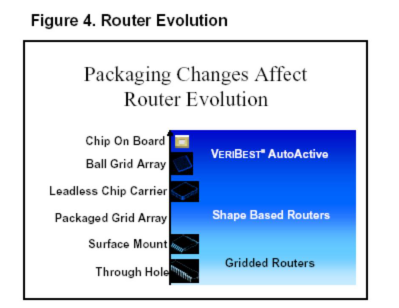
When the device was still in the through-hole insertion, grid router (girded-router) dominated the world. At that time, the vias were relatively large, the pin spacing was wide, and for most devices, the routing between the pads was very direct. With the advent of surface mount technology (SMT), the lead pitch began to shrink. The biggest advantages of surface mount technology at the time were smaller footprints and more pins (up to 84 per device). However, the pin pitch of the first surface mount device was 25 mils, which was gradually reduced to 11 mils. The minimum trace width and line spacing are also reduced correspondingly, which puts huge pressure on the existing routers. For the grid router, the smaller the grid, the slower its running speed. Eventually, mesh routers were replaced by mesh routers or shape-based routers. Bloodhound shape-based routers such as CCTSPECCTRA and Zuken-Redac were introduced in the mid-1990s. During this period, they experienced foot array packaging (PGA) and leadless chip carrier packaging (LCC), which have continued to the present. Facts have proved that in processing a variety of devices, different spacing, especially in processing fine-pitch devices, the gridless router is much better than the previous similar products.The shape-based router using the 90-degree angle algorithm is the most popular, and its performance has always been satisfactory. However, the good times are not long. With the advent of high-density, small-pitch mounting technology, some fundamental shortcomings of this type of 90-degree router are gradually exposed.
In the past few years, ball grid array packaging (BGA) and chip-scale/scale packaging (CSP) have swept the entire IC market. These two packages and several other packages such as flip-chip, multi-chip module (MCM), direct chip package (DCA), etc. are the most popular fine-pitch mounting technologies. Because the number of pins exceeds 500, chip manufacturers have adopted BGA packages, and the number of I/O (pins) has reached the highest record in history. The dense array of solder balls on the BGA far exceeds the I/O capacity of the traditional quad flat package (QFP). Because BGA has the characteristics of small size, good electrical performance, and low power consumption, designers and producers have always been fond of it. In 1998 alone, 42% of PCB designers claimed to use BGA packages, and this number is still growing. So far, the development of BGA technology has always been on the fast lane. The ball pitch of the early BGA package was 1.27mm, but the ball pitch of the current fine pitch ball grid array package (FPGBA) has been reduced to between 0.5-0.8mm.
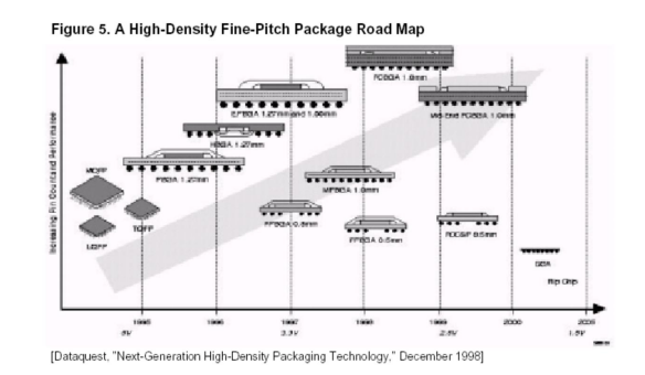
Chip size package (CSP) is another widely accepted and favored package form, especially in Japan. The small form factor and relatively reasonable cost of CSP make it useful in portable consumer electronics applications. According to Dataquest's survey, the CSP package is more suitable for those designs that need to mount low-pin count devices on small and high-density PCB boards.
Since the placement technology is very effective to meet the current market demand, it will continue to be the protagonist in the next few years and maintain the status of mainstream technology. It will also have a profound impact on printed circuit board wiring. In the transitional period of packaging technology upgrades, those routers that cannot smoothly cope with related problems will find it difficult to survive and can only be eliminated.
A large number of fine-pitch pins on a given component, the increasing number of components on the board, and the reduction in the overall size of the circuit board all make the challenges faced by current routers more difficult than ever. The smaller the pads, the smaller the trace width, and the tighter spacing, all bring trouble to the current 90-degree routing routers. The emergence of a large number of pin-interleaved devices has exacerbated the dilemma faced. In addition, 90-degree wiring cannot properly solve the most critical escape problem of the BGA package, and the required 45-degree vias cannot be made on the tightly-arranged solder ball pins.
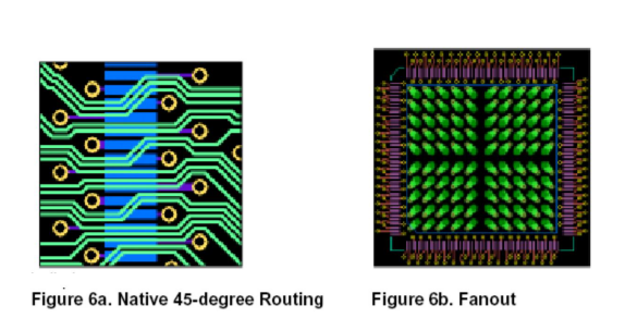
[Figure 6a.] Only true 45-degree wiring can give designers enough flexibility to cope with the dual problems of increased density and reduced area. In the picture, the router automatically runs multiple signal lines between the interleaved pins. [Figure 6b.] The sophisticated 45-degree angle large-area punching algorithm can perfectly solve the problem of BGA's way out. Dense vias and traces between pins are generally difficult to cross but can be squeezed by using the 45-degree wiring method. This algorithm must also be able to punch a large area of unconnected pins in order to adapt to the wide range of programmable devices.
Some 90-degree routers try to use the 45-degree angle as a post-processing process, but they actually become efficiency killers and reduce productivity. Because the entire circuit board is wired at a 90-degree angle from the beginning, designers cannot make optimal use of their own small board space. The lack of sufficient space usually impairs the performance of the router. Some other commonly used functions in high-speed design, such as the optimization of wiring corners, cannot be realized by 90-degree routers. In short, if you try to improve the 90-degree router to meet the current challenges, you must ultimately come at the expense of speed, performance, and compliance with high-speed design rules. In the end, it is the designer who suffers.
The ideal solution is a comprehensive, shape-based PCB design system that uses 45-degree wiring. The layout, intelligence, and automatic wiring of this system all run in the same environment and use the same editor. In this case, the designer actually only needs to punch a large area on the BGA footprint when routing, and then use the automatic routing device to quickly complete the task, and then optimize the overflow line according to the pre-established design rules. The big announcement was made. In the case of interactive modification, the 45-degree router will automatically include any changes made by the designer as required.
The market's demand for products with more functions, better performance, and smallest dimensions has prompted printed circuit board design to develop at an astonishing or even unimaginable speed. Obviously in this process, the traditional interconnection technology has been unable to adapt to the new generation of small-volume and high-density circuit design. The size of the through-hole is too large to be suitable for BGA and some other miniature high I/O pin devices. Increasing the number of layers of the board is not a wise choice. On the contrary, designers have tried their best to reduce the number of layers in response to the requirements of reducing production costs and shortening processing time. In order to obtain high-density wiring while reducing the number of layers, advanced fine-pitch interconnects seem to be the only way out. It can be seen that the challenge faced by PCB designers is undoubtedly to master the highly complex technology brought about by this technical solution. Of course, the router plays a pivotal role in it.
In the current dilemma, micro via technology finally came into being. Although micro-vias are now more expensive, they are very promising in the market. Therefore, while the increasing demand and the improvement of the process have led to the reduction of related processing costs, micro vias have attracted more and more attention. The extremely small miniature vias have naturally become the first choice for wiring design using BGA and CSP packages. The smallest through-hole size is 50um or 2mils inner diameter and 125um or 5mils outer diameter. The prevalence of miniature vias also makes blind and buried vias more widely used, which in turn facilitates the routing of high-density, array-type mounting devices. Many notable developments in processing and manufacturing have promoted the innovation of micro-vias, such as the combined manufacturing process pioneered in Europe and Japan, and the improvement of laser-plasma drilling processes.
One point is indisputable, that is, the PCB router must cover advanced connection characteristics to ensure the correct use of micro vias in the design. The new requirements include the use of vias between any two layers, and the aperture of each via is delayed. Supporting micro blind vias and buried vias is critical: a blind via connects the surface layer and one or more inner layers, while a buried via connects only the inner layer and the inner layer. In order to further reduce the wiring time and thereby shorten the overall design cycle, automatic wiring must also support micro-vias.
In order to maximize the wiring density, vias can be punched inside the pad, usually called via-under-pad or via-in-pad. For high-pin-count arrays, this method of punching is very practical when the pins are located in the center or inside the array. For the wrap-around pin distribution, it is almost impossible to complete the wiring work because the space is too crowded. In order to connect to the internal pin, the router must be able to automatically punch a via directly on the corresponding pad to allow the signal line to go from another layer, which also alleviates the space density problem on the top layer.
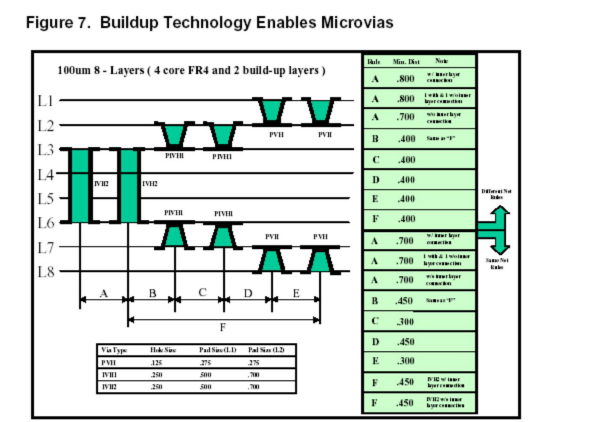
In this 8-layer board, the middle four layers or cores contain through holes, which are processed by traditional methods.
In this 8-layer board, the middle four layers or cores contain through holes, which are processed by traditional methods. On the contrary, the top and bottom layers are completed using image decomposition and sequential lamination methods. Circuit boards built in this way are widely used in computer, telecommunications, military, and aviation fields. This process is also applicable to multi-chip modules (MCMs).
You may interest in: What is Via in Pad in PCB Manufacturing
Still, need help? Contact Us: support@nextpcb.com
Need a PCB or PCBA quote? Quote now


 Surface

